
Instruction manual


Chapter 3
3-14
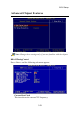
Configure SDRAM Timing by
Selects whether DRAM timing is controlled by the SPD (Serial Presence
Detect) EEPROM on the DRAM module. Setting to SPD enables SDRAM
Frequency, SDRAM CAS# Latency, Row Precharge Time, RAS Pulse
Width, RAS to CAS Delay and SDRAM Bank Interleave automatically to
be determined by BIOS based on the configurations on the SPD. Select-
ing User allows users to configure these fields manually.
SDRAM Frequency
Use this item to configure the clock frequency of the installed
SDRAM. Settings options:
For CPU FSB 100MHz SPD, HCLK, HCLK+33
For CPU FSB 133MHz SPD, HCLK, HCLK-33
SDRAM CAS# Latency
This controls the timing delay (in clock cycles) before SDRAM
starts a read command after receiving it. Settings: 2, 3 (clocks). 2
(clocks) increases the system performance the most while 3
(clocks) provides the most stable performance.
Row Precharge Time
This item controls the number of cycles for Row Address Strobe
(RAS) to be allowed to precharge. If insufficient time is allowed for
the RAS to accumulate its charge before DRAM refresh, refresh
may be incomplete and DRAM may fail to retain data. This item
applies only when synchronous DRAM is installed in the system.
Available settings: 2T, 3T.
RAS Pulse Width
This setting allows you to select the number of clock cycles
allotted for the RAS pulse width, according to DRAM
specifications. The less the clock cycles, the faster the DRAM
performance. Settings: 6T, 5T.
RAS to CAS Delay
This field allows you to set the number of cycles for a timing delay
between the CAS and RAS strobe signals, used when DRAM is