USERS MANUAL Revision 8.
TABLE OF CONTENTS Introduction................................................................................................................................................................................. 5 Overview ...................................................................................................................................................................................... 5 Specifications .............................................................................................
Output Selection for Sensors with Two Outputs ......................................................................................................................17 Timing........................................................................................................................................................................................ 18 Fixed Timing: .........................................................................................................................................
TABLE OF TABLES Table 1: Board Inputs, Outputs, Switches....................................................................................................................................22 Table 2: CCD Modes......................................................................................................................................................................23 Table 3: Binning Modes ...............................................................................................................
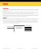
INTRODUCTION The Kodak Digital Science TM KAF Series CCD Digital Reference Evaluation Board provides a powerful platform to quickly and easily implement a Kodak Digital Science Full Frame or Blue Plus Full Frame CCD image sensor in a prototype imaging system. The Evaluation Board also serves as a useful reference design that will save considerable time and cost in the development of a product prototype.
SPECIFICATIONS Maximum Data Rate 6MHz Resolution 12 Bits Frame Rate Depends on Data Rate, CCD Array size, and Integration time. OUTPUTS: D[11..
ARCHITECTURE OVERVIEW A complete Block Diagram of the CCD Digital Reference Evaluation Board is shown in . MASTER CLOCK The Master Clock runs at eight times the Pixel clock frequency. The maximum pixel clock frequency is 6 MHz, which yields a maximum system clock frequency of 48 MHz. For slower Pixel clock frequencies, decrease the master clock frequency. The Default setting of the evaluation board is a 40 MHz system clock, with a pixel clock frequency of 5 MHz. The KAF-4301E is an exception to this.
CCD BIAS VOLTAGES CCD bias voltages (VRD, VOG, VLG) are supplied by filtered outputs of adjustable potentiometers. Fixed CCD bias voltages (LOD, VSS, GUARD) are supplied by filtered outputs of voltage dividers.
UNIT INTEGRATION TIME Integration Timing: The amount of time the CCD is exposed to light before clocking out the accumulated charge is called the integration time. An RC circuit and Schmitt trigger inverter are used to set the unit integration time. Total integration time is a multiple of the unit integration time. Altera Timing Rpot INTEGRATE C1 Set Unit Integration The circuit is set to toggle at 100 Hz, providing a fixed unit integration time of 10ms.
J1, J2 IMAGER BOARD CONNECTORS CCD Daughter Boards plug into these connectors. The daughter boards route the clock and bias traces from the timing board to the proper pins of the CCD. POWER SUPPLIES An onboard switching supply provides all of the voltages necessary to operate the CCD Digital Reference Evaluation Board, from a single +5V source. Switching supplies can, however, be a source of low-level asynchronous noise.
BOARD REQUIREMENTS: POWER SUPPLY The board requires only a single +5V, 1.5 Amp or greater power supply to operate. An on board switching power supply generates the necessary +15V, 120mA and –10V, 120mA power supplies from the 5V input. Although extensive filtering is done on board, the power supplied to the board must be quiet and stable in order to achieve the best possible performance. (See Power Supply Modes, for an alternative way to power the board.
CONFIGURATION MODES The following modes of operation are available to the user: LINE/SWITCHES MODES The Line/Switches Jumper (SW5) Selects whether some of the board settings will be controlled externally through the J6 connector (Line), or via the on-board switches (Switches). If this switch is set to Line, then the integration time and the binning mode must be set remotely via digital I/O. The still/free-run mode switch (SW3, 3-position switch) can also be set externally when the Line mode is selected.
AD_IN/EX MODES The board comes with an Analog Devices AD9816 12 bit A/D converter on board. This A/D has several features, such as multiple configurations, programmable gain, and offset registers which require initialization and/or programming on power up. The programming of these registers is done via a three wire serial interface.
ADJUSTMENTS Adjustments can be made to the A/D registers during operation of the board by utilizing the DATA dipswitch (SW10), the ADDRESS switch (SW9), and the Image_Acquire control line. After setting SW9 to the desired Address, and SW10 to the desired Data, send an Image_Acquire signal either by pressing the Image_Acquire button or remotely via the J6 connector control line.
POWER SUPPLY MODES Power can be supplied to the board in one of two ways: Switching Power Supply The board comes supplied with a 500 kHz switching power supply (Linear Technologies LT1372). If it is desired to utilize the on-board switching supply, the board should be configured as follows: 1. Connect a 5V, 1.5A or greater lab supply to the J5 power connector. 2. Install Jumper 6 and Jumper 4. 3. Remove Jumper 7 and Jumper 5. 4. Set Jumper 1 to the ON position.
CCD IMAGER BOARDS Each CCD has an imager board. The imager boards route the bias voltage traces from the timing board through connectors J1 and J2 to the appropriate pins on the device. The imager boards contain the Horizontal and Reset clock driver ICs as well as the emitter-follower circuit that buffers and drives the video signal down to the timing board. ADJUSTMENTS Fixed Bias Voltages: Fixed Voltages: VDD +15V LOD/GUARD +10V VSUB 0V VSS 0 to +2.
OUTPUT SELECTION FOR SENSORS WITH TWO OUTPUTS The KAF-1001E, KAF-0261E, and KAF-4301E sensors have two video outputs. The outputs have different gain and one of them is selected depending on the application. The imager daughter boards for these sensors have two jumpers that must be set correctly to enable the desired output.
TIMING FIXED TIMING: H1, H2 VARIABLE TIMING: V1, V2 (binning modes) RESET (binning modes) CLAMP (binning modes) SAMPLE (binning modes) A/D Clock (binning modes) See Timing Diagram 1 – Figure 4: Pixel Rate Timing See Timing Diagram 3 -Figure 12: Binning Mode Timing (2x2 binning shown) Note: Not available with the KAF-16801E, KAF-16801LE and KAF-4301E image sensors.
FIGURES, TABLES, TIMING DIAGRAMS, AND PERFORMANCE DATA J5 +5V 7414 C 10uF -18V J8 R 1K -10V +18V Unit Integration Time +5V +15V LT1372 Switching Supply 10 pin JTAG Header Power_on_clear J6 34 pos VDD VRD J1 24 position connector Vclks Driver CCD Daughter Board Altera 7000S PLD 2 Capture Button Hclks Driver CCD Sensor Rclk Driver 8 bit Line Drivers Still/FreeRun Int[5..0] Bin[2..
CLOCKING STATE MACHINE Power ON CLEAR_ALL CLOCK = EIGHTH CLOCK SET-UP RESET = POWER ON CLEAR INITIALIZE STILL/FREERUN? NO STILL IMAGE ACQUIRE? FREE-RUN YES INTEGRATION FLUSH INTEGRATION_DONE V_TRANSFER V_ENABLE H_TRANSFER V_XFER_DONE = LOW H_XFER_DONE LINE_CHECK V_XFER_DONE = HIGH Figure 2: Clocking State Machine ©Eastman Kodak Company, 2008 www.kodak.com/go/imagers Revision 8.
Address Register Function 0 Configuration Register bit 7 MSB bit 6 bit 5 Default Programming 1 2 3 4 5 6 7 bit 4 bit 3 bit 2 bit 1 bit 0 MUX Register bit 7 bit 6 bit 5 bit 4 bit 3 bit 2 bit 1 bit 0 Red PGA Register Green PGA Register Blue PGA Register Red Offset Register Green Offset Register Blue Offset Register test mode bit test mode bit CDS mode bit input span input span channel mode channel mode test mode bit test mode bit channel sequence channel sequence channel select channel select channel
Switches Inputs Line/Switches Select where control of modes comes from Switch_Int[5..0] Switch_Bin[2..0] Switch_CCD[3..0] Still/Free-Run A/D_in/ex Sync_test_pix/line Sync_test_enable Integration timing control lines Binning mode control lines Device Select (KAF 0400, KAF1600 ...
CCD Switch Setting CCD Pixels/Line Lines/Frame 0* 1 2 3 4 5 6 7 8 9 A B C Test Mode1 or KAF-16801E/LE KAF-1401E Test Mode 2 KAF-1301E, KAF-1301LE KAF-4202 KAF-1602E, KAF-1602LE KAF-6303E, KAF-6302LE KAF-0401E, KAF-0401LE KAF-3200ME KAF-1001E KAF-0261E KAF-16800 KAF-4301E 100 1500 10 1500 2300 1700 3300 1000 2300 1200 700 4300 2300 2 1200 4 1200 2150 1100 2150 650 1600 1150 650 4200 2200 Table 2: CCD Modes Note: In order to operate the KAF-16801E/LE sensor using the KAF Series CCD Digital Reference
Bin Switch (SW2) Setting Binning Mode 1 2 3 4 5 6 7 0 1x1 (No Binning) 1x1 (No Binning) 1x1 (No Binning) 1x1 (No Binning) 1x1 (No Binning) 1x1 (No Binning) 1x1 (No Binning) 1x1 (No Binning) Table 4: Binning Modes when Configured for use with the KAF-16801E/LE Note: In order to operate the KAF-16801E/LE sensor using the KAF Series CCD Digital Reference Evaluation Board, the board is configured with a unique PLD program.
SW7 Switch Setting INT 5-3 Switch Integration Time (Coarse) (Coarse) (Seconds) 0 1 2 3 4 5 6 7 000 001 010 011 100 101 110 111 0 1 2 3 4 5 7 9 SW6 Switch Setting Integration Time (Fine) INT 2-0 Switch Setting Fine 0 1 2 3 4 5 6 7 000 001 010 011 100 101 110 111 0* 20 50 100 200 300 500 800 (ms) Table 6: Integration Time Modes Note: If both SW7 and SW6 are set to zero, the integration time is set to 10ms. ©Eastman Kodak Company, 2008 www.kodak.com/go/imagers Revision 8.
Vdark+Voffset Vsat Vpix Video 1 count = 8t 1t Reset H1 8t H2 1t Clamp 3t Sample 4t A/D clock 3t PIX t = 1/system clock (Default Setting = 200ns) Figure 4: Pixel Rate Timing Note: The KAF-4301E implements 16t = 1pixel and 32t = 1 pixel modes instead of the 8t=1pixel timing. This provides pixel frequencies of 2.5 MHz and 1.25 MHz. ©Eastman Kodak Company, 2008 www.kodak.com/go/imagers Revision 8.
Integration Time 64 t 64 t 64 t 5t V1 V2 LINE* 140t 2t FRAME* 12t 50t 25t H1 222t H2 R Clamp Sample A/D clk PIX* t = 1/system clock (Default Setting = 200ns) Figure 5: Line Rate Timing for KAF-0261E, 0402E, 1001E, 1301E, 1402E, Note: The line rate timing for the KAF-4301E is similar to this with the addition of an overlap period in the vertical clock timing. Consult the current specification for the KAF-4301E for details. ©Eastman Kodak Company, 2008 www.kodak.com/go/imagers Revision 8.
Integration Time 100 t 100 t 100 t 4t V2 V1 LINE* 248t 2t FRAME* 50t 25t H2 329t H1 R Clamp Sample A/D clk PIX* t = 1/system clock (Default Setting = 200ns) Figure 6: Line Rate Timing for KAF-16801E/LE Sensors ©Eastman Kodak Company, 2008 www.kodak.com/go/imagers Revision 8.
Frame Timing (KAF 0261,0401,1001,1302,1401,1602,2001,4202,4300,6303,16800) Integration Time tReadout 1 Frame = N Lines V1 V2 Line 0 1 N-1 N LINE* FRAME* H1 H2 R Clamp Sample A/D clk PIX* Figure 7: Frame rate timing for the KAF-0261E, 0402E, 1001E, 1301E, 1402E, Note: Default Frame Grabber Settings ©Eastman Kodak Company, 2008 www.kodak.com/go/imagers Revision 8.
Frame Timing (KAF3040, KAF 3200) Integration Time tReadout 1 Frame = N Lines V2 V1 Line 0 1 N-1 N LINE* FRAME* H2 H1 R Clamp Sample A/D clk PIX* Figure 8: Frame Timing for the KAF-3200ME Sensor ©Eastman Kodak Company, 2008 www.kodak.com/go/imagers Revision 8.
Vdark+Voffset Vsat Vpix Video 1 count = 8t 1t Reset H2 8t H1 Clamp 1t 3t Sample 4t A/D clock 3t PIX t = 1/system clock (Default Setting = 200ns) Figure 9: Pixel Rate Timing for the KAF-3200ME, KAF-16801E, KAF-16801LE Sensors ©Eastman Kodak Company, 2008 www.kodak.com/go/imagers Revision 8.
Still Mode: Flush and Integration Timing Flush Timing IMAGE ACQUIRE CCD Readout Time Integration Time T = 128t 5t 5t 66t** V1 Line 0 V2 Line N 4000 T INTEGRATE LINE* 7t FRAME* PIX* Figure 10: Still Mode: Flush and Integration Timing Free Run Mode: Integration Timing CCD Readout Time CCD Readout Time Integration Time Frame N 1 Frame = N Lines Frame N+1 1 Frame = N Lines INTEGRATE 5t V1 Line N-1 V2 Line N Line 0 Line 1 3t LINE* 7t FRAME* PIX* Figure 11: Free Run Mode: Integration Timi
Vpixbinned Video 1 count = 8*(bin mode)*t 1t t = 1/system clock (Default Setting =200ns) Reset H1 8t H2 1t Clamp 3t Sample 4t A/D clock 3t PIX Pixel Rate Timing Figure 12: Binning Mode Timing (2x2 binning shown) In Binning Modes, the Frequency of the Reset, Clamp, Sample, A/D, and PIX clocks are decreased in order to allow charge to accumulate on the output node of the CCD before being reset.
Linearity 18 000 0 16 000 0 Electron s 14 000 0 12 000 0 10 000 0 Li ne arity Cu rve 80 000 60 000 Fu ll Wel l = 11 500 0 Ele ctrons 40 000 20 000 0 0 20 00 40 00 60 00 80 00 10 000 Integration Time (ms) Figure 13: Measured Linearity (Measurements taken using KAF-1600 sensor) Photon Transfer Curve (5MHz, Gain = 2.5) Noise (A/D Counts) 10 00 10 0 Sl op e = El/ADU = 2 9.2 el ectron s No ise Fl oor = 1.
SYSTEM NOISE FLOOR VS. OPERATING FREQUENCY Frequency Noise Floor Dynamic Range* Dynamic Range* El/ADU System Gain (MHz) (Electrons) (Bits) (dB) 1 40 11.49 69.17 29.2 2.5X 2 48 11.23 67.59 29.2 2.5X 3 50 11.17 67.23 29.2 2.5X 4 54 11.06 66.57 29.2 2.5X 5 56 11.00 66.25 29.2 2.5X 6 58 10.95 65.95 29.2 2.
Linearity of Programmable Analog Gain 800 A/D Units 600 400 200 0 0 15 30 45 60 75 90 105 120 135 150 165 180 195 210 225 240 255 Programmable Gain Code Measured Gain PGA Gain 7 6 5 4 3 2 1 0 0 15 30 45 60 75 90 105 120 135 150 165 180 195 210 225 240 255 Programmable Gain Code 1.1 Incremental Gain 1.05 Ideal Delta = 1.019 1 Measured 0.95 0.
CONNECTOR PINOUTS Imager Board Connectors J1, J2 Connector Pin Assignment Connector Pin Assignment J1 1 N.C. J2 1 VSUB J1 2 VSUB J2 2 RESET J1 3 N.C. J2 3 VSUB J1 4 VSUB J2 4 N.C. J1 5 N.C. J2 5 VSUB J1 6 VSUB J2 6 N.C. VSUB J1 7 VLG J2 7 J1 8 VSUB J2 8 N.C. J1 9 N.C. J2 9 VSUB J1 10 VSUB J2 10 N.C. J1 11 VDD J2 11 VSUB J1 12 VSUB J2 12 H2 J1 13 VDD J2 13 VSUB J1 14 VSUB J2 14 H1 J1 15 N.C.
Input Connector J6 ©Eastman Kodak Company, 2008 Pin Assignment Pin Assignment 1 INT0 2 GND 3 INT2 4 GND 5 INT3 6 GND 7 INT5 8 GND 9 IMAGE_ACQUIRE 10 GND 11 BIN0 12 GND 13 BIN1 14 GND 15 SCLOCK 16 GND 17 INT1 18 GND 19 SLOAD 20 GND 21 INT4 22 GND 23 BIN2 24 GND 25 SDATA 26 GND 27 STILL/FREE-RUN 28 GND 29 N.C. 30 GND 31 N.C. 32 GND 33 N.C. 34 GND www.kodak.com/go/imagers Revision 8.
Output Connector J4 ©Eastman Kodak Company, 2008 Connector Pin Assignment Comment J4 1 DIG0+ RS422 J4 2 DIG0- RS422 J4 3 DIG1+ RS422 J4 4 DIG1- RS422 J4 5 GND J4 6 DIG2+ RS422 J4 7 DIG2- RS422 J4 8 DIG3+ RS422 J4 9 DIG3- RS422 J4 10 GND J4 11 DIG4+ RS422 J4 12 DIG4- RS422 J4 13 DIG5+ RS422 J4 14 DIG5- RS422 J4 15 GND J4 16 DIG6+ RS422 J4 17 DIG6- RS422 J4 18 DIG7+ RS422 J4 19 DIG7- RS422 J4 20 GND J4 21 DIG8+ RS422 J4 22
Integrate Sync Connector J7 Connector Pin Assignment Comment J7 J7 1 2 Integrate GND TTL Connector Pin Assignment J5 J5 J5 J5 J5 1 2 3 4 5 +18V SUPPLY GND -18V SUPPLY GND +5V Connector Pin Assignment J8 J8 J8 J8 J8 J8 J8 J8 J8 J8 1 2 3 4 5 6 7 8 9 10 TCK GND TDO +5V TMS N.C. N.C. N.C. TDI GND Power Connector J5 JTAG Connector J8 ©Eastman Kodak Company, 2008 www.kodak.com/go/imagers Revision 8.
REFERENCES Analog Devices AD9816 Specification Sheet Linear Technology LT1372 Specification Sheet KAF Series Device Performance Specifications ISS Application Note on KAF Series Binning Mode Operation (DS 02-009) ORDERING INFORMATION The Kodak Digital Reference Evaluation Board may be ordered directly from: Eastman Kodak Company, Image Sensor Solutions Rochester, NY 14650-2010 Tel. No. (585) 722-4385 Fax No. (585) 477-4947 Web: http://www.kodak.com/go/imagers E-mail: imagers@kodak.
APPENDIX APPENDIX1: PART NUMBER AVAILABILITY Note: This appendix may be updated independent of the performance specification. Contact Eastman Kodak Company for the latest revision.
APPENDIX 2: PARTS LIST PART DESCRIPTION PACKAGE QTY. BOARD REFERENCE # MANUFACTURER BLM11P600SPT FERRITE FERRITE 0603 51 FB1-15, FB17-18, FB20-53 MURATA ERIE 06035A151JAT2A 150pF 50VDC CAP 0603 1 C62 AVX 06035C102KAT4A 1000pF 50VDC CAP 0603 3 C9, C43-44 AVX 08055A122KATMA 1200pF 50VDC CAP 0805 3 C29, C91-92 AVX 06035C103KAT4A .01uF 50VDC CAP 0603 36 AVX 0603YC104MAT4A .1uF 16V CAP 0603 13 12063E334MATMA 0.
CRCW0603-1002-FT 10K OHM 1% RES 0603 25 4310R-101-103 10K SIP 10 POS THRU 1 R1-5, R20, R24-27, R30-31, R48, R52, R61-62, R64, R68, R70, R72-76, R78 R28 DALE 3266W-1-103 10K POT THRU-HOLE 4 R11-13, R67 BOURNS 3296W-1-503 50K POT THRU-HOLE 1 R6 BOURNS CRCW0603-6982-FT 69.8K OHM 1% RES 0603 1 R33 DALE CRCW0603-8062-FT 80.
5-826632-0 BREAKAWAY STRIP HEADER 24 2 J1,J2 AMP 5-826632-0 BREAKAWAY STRIP HEADER 10 1 J8 AMP 5-826632-0 BREAKAWAY STRIP HEADER 2 1 J7 AMP 5-826632-0 BREAKAWAY STRIP JUMPER 9 AMP 5-826926-0 BREAKAWAY STRIP TEST POINT 27 JMP1, JMP3-7, SW4-5, SW11 TP1, TP4-5, TP10, TP12, TP14-17, TP22, TP24-28, TP31-39, TP44-46 ©Eastman Kodak Company, 2008 www.kodak.com/go/imagers AMP Revision 8.
APPENDIX 3: IMAGER BOARD SCHEMATICS ©Eastman Kodak Company, 2008 www.kodak.com/go/imagers Revision 8.
This page intentionally left blank. ©Eastman Kodak Company, 2008 www.kodak.com/go/imagers Revision 8.
©Eastman Kodak Company, 2008. Kodak and Pixelux are trademarks.