
User's Manual


Chapter 1 – Universal Socket Connectivity
Multi-Tech Systems, Inc. Universal Socket Hardware Guide for Developers (S000342G) 5
Design Considerations
Noise Suppression Design Considerations
Engineering noise-suppression practices must be adhered to when designing a printed circuit board (PCB)
containing the SocketModem module. Suppression of noise is essential to the proper operation and
performance of the modem itself and for surrounding equipment.
Two aspects of noise in an OEM board design containing the SocketModem must be considered: on-
board/off-board generated noise that can affect digital signal processing. Both on-board and off-board
generated noise that is coupled on-board can affect interface signal levels and quality. Of particular concern
is noise in frequency ranges affecting modem performance.
On-board generated electromagnetic interference (EMI) noise that can be radiated or conducted off-board is
a separate, but equally important, concern. This type of noise can affect the operation of surrounding
equipment. Most local government agencies have stringent certification requirements that must be met for
use in specific environments.
Proper PC board layout (component placement, signal routing, trace thickness and geometry, etc.)
component selection (composition, value, and tolerance), interface connections, and shielding are required
for the board design to achieve desired modem performance and to attain EMI certification.
Other aspects of proper noise-suppression engineering practices are beyond the scope of this designer
guide. The designer should consult noise suppression techniques described in technical publications and
journals, electronics and electrical engineering text books, and component supplier application notes.
PC Board Layout Guidelines
In a 4-layer design, provide adequate ground plane covering the entire board. In 4-layer designs, power and
ground are typically on the inner layers. All power and ground traces should be 0.05 inches wide.
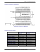
The recommended hole size for the SocketModem pins is 0.036 in. +/-0.003 in. in diameter. Spacers can be
used to hold the SocketModem vertically in place during the wave solder process. A spacer should be
placed on pin 32 and pin 64 of the SocketModem. A suggested part number for the spacer is BIVAR 938-
0.130 for P1 (0.310in) option SocketModems. The spacers can be left on permanently and will not effect
operation.
All creepages and clearances for the SocketModem have been designed to meet requirements of safety
standards EN60950 or EN60601. The requirements are based on a working voltage of 125V or 250V. When
the recommended DAA* circuit interface is implemented in a third party design, all creepage and clearance
requirements must be strictly followed in order to meet safety standards. The third party safety design must
be evaluated by the appropriate national agency per the required specification.
User accessible areas: Based on where the third party design is to be marketed, sold, or used, it may be
necessary to provide an insulating cover over all TNV exposed areas. Consult with the recognized safety
agency to determine the requirements.
Note: Even if the recommended design considerations are followed, there are no guarantees that a
particular system will comply with all the necessary regulatory requirements. It is imperative that specific
designs be completely evaluated by a qualified/recognized agency.
*DAA stands for Data Access Arrangement. DAA is the telephone line interface of the module.