
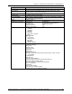
Specifications
Chapter 3 – SocketModem (MT5634SMI-34 & MT5634SMI-92)
Multi-Tech Systems, Inc. Universal Socket Hardware Guide for Developers (S000342C) 68
Electrical Characteristics
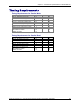
3.3 V Serial – Industrial Temperature (SMI-ITP) Build Option
3.3 V DC Characteristics (TA = -40 °C to 85 °C; VDD = 3.3 V ± 0.3 V) VDDMAX = 3.6 V
Digital Inputs
–DTR (40), –TXD (35), –RTS (33)
Input High
Min 2.52 V
Input Low
Max 0.9 V
–Reset (24) Input High
Min 2.52 V
Input Low
Max 0.3 V
Digital Outputs
–DCD (39), –CTS (38), –DSR (37), –RI (36), –RXD (34)
Output High
Min. 2.3 V
Output Low
Max 0.4 V
Current Drive
2 mA
Digital Input Capacitance
5 pF
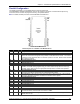
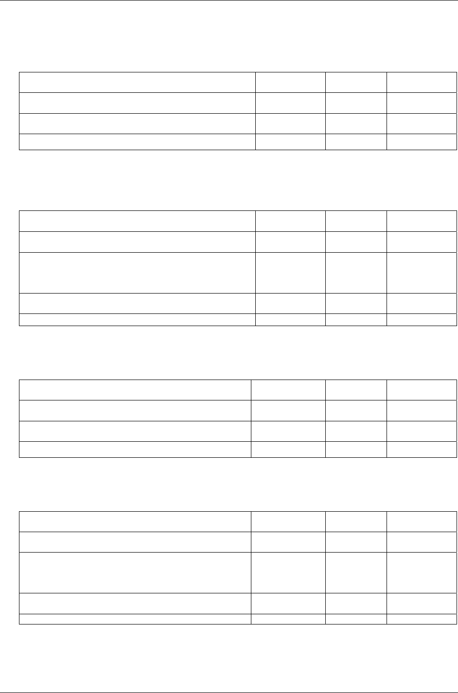
3.3 V Parallel – Standard (SMI) and Industrial Temperature (SMI-ITP) Build Options
MT5634SMI for Parallel MT5634SMI SocketModem devices are presented below.
3.3 V DC Characteristics (TA = –40 °C to 85 °C; VDD = 3.3 V ± 0.3 V)
VDDMAX = 3.6 V
Digital Inputs
–DS (40)
Input High
Min 2.52 V
Input Low
Max 0.9 V
Digital Inputs (hysteresis input buffer)
A0 (31), A1 (25), A2 (34), –WR (32), –RD (33)
Input High
Min 2.52 V
Input Low
Max 0.9 V
Digital Input/Output
Output buffer can source 12 mA at 0.4 V
DO (37), D1 (38), D2 (29), D3 (39), D4 (35), D5 (36), D6
(41), D7 (27)
Input High
Min 2.52 V
Input Low
Max 0.9 V
Digital Output
INT (30)
Output High
Min 2.3 V
Output Low
Max 0.4 V
Current Drive
2 mA
Digital Input Capacitance 5 pF
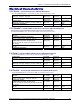
5 V Serial – Standard (SMI) and Medical Device (SMI-HV) Build Options
5 V DC Characteristics (TA = 0 °C to 50 °C; VDD = 5 V ± 0.25 V) VDDMAX = 5.25 V
Digital Inputs
–DTR (40), –TXD (35), –RTS (33)
Input High
Min 3.675 V
Input Low
Max 1.4 V
–Reset (24) Input High
Min 3.675 V
Input Low
Max 0.3 V
Digital Outputs
–DCD (39), –CTS (38), –DSR (37), –RI (36), –RXD (34)
Output High
Min. 4 V
Output Low
Max 0.4 V
Current Drive
2 mA
Digital Input Capacitance
5 PF
5 V Parallel – Standard (SMI) and Medical Device (SMI-HV) Build Options
5 V DC Characteristics (TA = 0 °C to 50 °C; VDD = 5 V ± 0.25 V) VDDMAX = 5.25 V
Digital Inputs
–DS (40)
Input High
Min. 3.675 V
Input Low
Max. 1.4 V
Digital Inputs (hysteresis input buffer)
A0 (31), A1 (25), A2 (34), –WR (32), –RD (33)
Input High
Min. 3.675 V
Input Low
Max. 1.4 V
Digital Input / Output
Output buffer can source 12 mA at 0.4 V
DO (37), D1 (38), D2 (29), D3 (39), D4 (35), D5 (36), D6
(41), D7 (27)
Input High
Min. 3.675 V
Input Low
Max. 1.4 V
Digital Output
INT (30)
Output High
Min. 4 V
Output Low
Max 0.4 V
Current Drive
2 mA
Digital Input Capacitance 5 pF