
Data Sheet


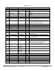
Table Of Contents
- Revision History
- Table of Contents
- 1 Introduction
- 2 Mechanical Specification
- 3 DC Electrical Specification
- 4 RF Specification
- 5 Environmental Specification
- 6 Power Sequence
- 7 Application Information
- 8 Application Reference
- 9 Assembly Information
- 10 Packaging and Marking Information
- 11 Regulatory Information
- 12 RoHS Information
- 13 Ordering Information
- 14 Notice
- 15 Preconditions To Use Murata Products

Copyright © Murata Manufacturing Co., Ltd. All rights reserved. October 2017
MBN52832 Data Sheet, v1.3, 11/13/2018 Page 10 of 34 www.murata.com
Table 2.2 Pinouts
Pin #
Pin Name
Nordic IC Pin
I/O
Description
1
P0_09/NFC ANT
P0.09/NFC
I/O
GPIO; NFC antenna connection.
2
P0_06
P0.06
I/O
GPIO
3
P0_00/XL1
P0.00/XL1
I/O
Connection for 32.768kHz crystal (LFXO);
GPIO
4
P0_01/XL2
P0.01/XL2
I/O
Connection for 32.768kHz crystal (LFXO);
GPIO
5
GND
GND
6
VCC
VDD
Module power supply
7
DCC
DCC
DC/DC converter output pin. *Refer to
reference schematic.
8
DEC
DEC4
1V3 regulator supply decoupling. Input from
DC/DC converter. Output from 1.3V LDO.
*Refer to reference schematic.
9
P0_02/AIN0
P0.02/AIN0
I/O
GPIO; SAADC/COMP/LPCOMP input
10
P0_05/AIN3
P0.05/AIN3
I/O
GPIO; SAADC/COMP/LPCOMP input
11
P0_03/AIN1
P0.03/AIN1
I/O
GPIO; SAADC/COMP/LPCOMP input
12
P0_04/AIN2
P0.04/AIN2
I/O
GPIO; SAADC/COMP/LPCOMP input
13
P0_29/AIN5
P0.29/AIN5
I/O
GPIO; SAADC/COMP/LPCOMP input
14
P0_07
P0.07
I/O
GPIO
15
P0_08
P0.08
I/O
GPIO
16
SWDIO
SWDIO
I/O
Serial Wire Debug I/O for debug and
programming.
17
P0_21/RESET
P0.21/RESET
I/O
GPIO; Configurable as system RESET pin
18
SWDCLK
SWDCLK
I/O
Serial Wire Debug clock input for debug
and programming.
19
GND
GND
GND
20
ANTIN
*Refer to reference schematic.
21
ANTOUT
RF signal output. Connect to ANTIN for on-
board antenna or to external antenna.
*Refer to reference schematic.
22
P0_18/TRACE0
P0.18/TRACE
DATA[0]
I/O
GPIO; Trace port output;
23
P0_16/TRACE1
P0.16/TRACE
DATA[1]
I/O
GPIO; Trace port output.
24
P0_15/TRACE2
P0.15/TRACE
DATA[2]
I/O
GPIO; Trace port output.
25
P0_14/TRACE3
P0.14/TRACE
DATA[3]
I/O
GPIO; Trace port output.
26
P0_10/NFC ANT
P0.10/NFC
I/O
GPIO; NFC antenna connection.
27
P0_20
P0.20
I/O
GPIO
28
P0_17
P0.17
I/O
GPIO
29
P0_13
P0.13
I/O
GPIO
30
GND
Ground.
31
GND
Ground.
32
GND
Ground.
33
GND
Ground.