500M Module and Daughter Card Data Sheet 500M is Itron’s second generation modular modem that enables rapid development and deployment of Smart Utility and Smart City applications anywhere. 9 August 2021 815-0444-00 REV 001 Itron, Inc.
500M Module and Daughter Card Data Sheet Copyright 500M and Daughter Card Data Sheet 9 August 2021 815-0444-00 Copyright © 2021 Itron, Inc. All rights reserved. Confidentiality Notice The information contained herein is proprietary and confidential and is being provided subject to the condition that (i) it be held in confidence except to the extent required otherwise by law and (ii) it will be used only for the purposes described herein.
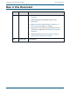
500M Module and Daughter Card Data Sheet Contents Contents Copyright ................................................................................................................................................ 2 Contents ................................................................................................................................................. 3 New in this Document ....................................................................................................................
500M Module and Daughter Card Data Sheet 2.3. Contents Connector Locations............................................................................................................ 23 2.3.1. Connector Functions and Locations .......................................................................... 24 3. Reliability and Regulatory Certification ........................................................................................... 28 3.1. 3.2. FCC/ISED Regulatory Integration Instructions ......
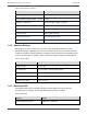
00M Module and Daughter Card Data Sheet New in this Document New in this Document Revision Date 001 August 9, 2021 000 August 9, 2021 October 2020 Description Added 500M Antenna to 500M Family Products Ordering Information Updated Modulation and Data Rates rows in Radio Specifications Moved PCB Design Guidelines and Transmission Line Measurements from Chapter 3 to Chapter 1 Removed the section called "FCC and ISED Government Guidelines" and replaced it with Reliability and Regulator
500M Module and Daughter Card Data Sheet 500M Module 1. 500M Module 1.1.
500M Module and Daughter Card Data Sheet 500M Module Real-time clock (RTC) Physical (PHY) layer and Media Access Control (MAC) protocol stack RF transceiver with power amplifier Filters and matching circuitry Communications processor Figure 1 500M component diagram Note: The Device IC described in the figure above is an external device to which the 500M can interface. 1.2.1.
500M Module and Daughter Card Data Sheet 500M Module Catalog Number Product 155-0200-00 500M Antenna (model WPANT30182-R1A) 1.3. Features The 500M module features a Land Grid Array (LGA) footprint and is designed to be compatible with harsh environment potted and non-potted applications. Table 2 describes the 500M’s main features.
500M Module and Daughter Card Data Sheet 500M Module Table 3 Normal operating conditions Feature Description Supply Voltage – nominal 2.55VDC Power Amplifier Supply Voltage – nominal 3.0VDC Voltage on Analog Pins 0 to VCC (supply voltage - nominal) Operating Relative Humidity 5% to 95% RH non-condensing (shall be washed) Transmit Current 430 mA max typical at 3V at 27 dBm Receive Current 25mA typical (at 2.55V) Processor-only current 4.5 mA typical (at 2.
500M Module and Daughter Card Data Sheet 500M Module Feature Rating ESD Suppression antenna pins Charged device model: 250V Human Body Model The Human Body model (HBM) simulates discharge between a human (hand/finger) and conductor (metal rail). The 500M HBM rating is Class 0 (<250V). Itron recommends that the appropriate ESD handling precautions are taken.
500M Module and Daughter Card Data Sheet 500M Module Figure 2 Utilization of power domains 1.4.5. Data Connection High-Level Data Link Control (HDLC) is the link layer protocol that is used over the serial connection between the host processor and the 500M. Application layer messages encoded as Constrained Application Protocol (CoAP) Protocol Data Units (PDUs) are sent over this interface.
500M Module and Daughter Card Data Sheet 500M Module 1.5.1. Package Drawing and Pad Diagram Figure 3 Top shield laser etchings Figure 4 Package and pad identifier drawing 1.5.2. Connector Functions and Locations The following table describes the PIN numbers, name, and other useful information. Table 7 Pin numbers and names August 9, 2021 815-0444-00 REV 001 Itron, Inc.
500M Module and Daughter Card Data Sheet 500M Module PIN Number Function PIN name Input/Output Description 4 Standard Interface UART4_TX PA0 Output Serial UART interface (up to 115,200 bps, 8-N1) 5 UART4_RX PA1 Input Serial UART interface (up to 115,200 bps, 8-N1) 47 UART4_WAKE PA15 Input Interrupt pin - wake up 500M so host processor can send data 8 LPUART1_TX PA2 Output Serial UART interface (up to 115,200 bps, 8-N1) 9 LPUART1_RX PA3 Input Serial UART interface (up to 115,200 bp
500M Module and Daughter Card Data Sheet PIN Number Function 500M Module PIN name Input/Output Description PB14 I/O NC I2C2_SCL USART3_CTS 19 SPI2_MISO I2C2_SDA USATR3_RTS 18 SPI2_MOSI PB15 I/O NC 6 SPI2_SS# (IRQ3) PC3 I/O NC 56 I2C4_SDA/I2C3_SDA PC0 I/O NC 57 I2C4_SCL/I2C3_SCL PC1 I/O NC 10 USART3_TX PC4 Output NC 12 USART3_RX PC5 Input NC EN_VRF PC6 Output Enable RF Power DC/DC SYNC/MODE PC7 Output Enable Power Supply 25 PWRGD_VPA PC8 GND RF Ground 35 LF_CLK
500M Module and Daughter Card Data Sheet PIN Number Function 500M Module PIN name Input/Output Description 3 GND Power Ground 7 GND Power Ground 11 GND Power Ground 14 GND Power Ground 16 GND Power Ground 17 GND Power Ground 22 GND Power Ground 26 GND Power Ground 30 GND Power Ground 31 GND Power Ground 32 GND Power Ground 33 GND Power Ground 34 GND Power Ground 39 GND Power Ground 40 GND Power Ground 41 GND Power Ground 46 GND Power
500M Module and Daughter Card Data Sheet 500M Module Standard Moisture/Reflow Sensitivity Classification for NonHermetic Solid State Surface Mount Devices. If the 500M is not mounted to a circuit board within 72 hours – the maximum “out of bag” or floor life exposure time – then the module must be baked in accordance with IPC/JEDEC J-STD-033, Handling, Packing, Shipping and Use of Moisture, Reflow, and Process Sensitive Devices to remove any moisture absorbed.
500M Module and Daughter Card Data Sheet 500M Module Feature Description Data Rates 10 kbps, 25 kbps, 50 kbps, 100 kbps, 150 kbps, 300 kbps, 16.384 kbps Receiver Sensitivity -114 dBm at 10 kbps Receiver sensitivity depends on communications protocol and data rate. The table above describes typical measured receive sensitivity, assuming 10% packet error rate (PER) and 250-byte payload. 1.7.
500M Module and Daughter Card Data Sheet 500M Module speed digital signals, near the transmission line. Locate the transmission line trace away from power supply lines and power supply regulation circuitry. 1.7.2. Key Design Parameters The antenna trace must have a characteristic impedance of 50 Ω +/- 5%. The recommended dimensions and the Gerber layout for the antenna trace are provided on the following pages. Transmission line parameter calculations are required for calculating the key parameters.
500M Module and Daughter Card Data Sheet 500M Module Figure 6 PCB Stackup Figure 7 Coplanar waveguide with ground outline and vias spaced at 50mils Figure 8 Coplanar waveguide with Full ground pour August 9, 2021 815-0444-00 REV 001 Itron, Inc.
500M Module and Daughter Card Data Sheet 500M Module 1.8. Transmission Line Measurements For design verification, use of an S-Parameter Network Analyzer, such as Agilent 8719S may be used to characterize the losses of the transmission line. Solder a calibrated coaxial cable to pin 43 (RF900, RF I/O port) on the PCB to make the following measurements. Figure 9 S21 Path Loss Figure 10 S11_impedance_measurement August 9, 2021 815-0444-00 REV 001 Itron, Inc.
500M Module and Daughter Card Data Sheet 500M Module 1.8.1. External Antenna Integration (RSS-GEN) This radio transmitter has been approved by Innovation, Science and Economic Development (ISED) Canada to operate with the antenna type with the maximum permissible gain and required antenna impedance for each antenna type indicated. Antenna types that are not described are strictly prohibited for use with this device because they have a gain greater than the maximum gain indicated for that type.
500M Module and Daughter Card Data Sheet 500M Daughter Card 2. 500M Daughter Card The 500M module is available in a Daughter Card form factor with power regulator and MMCX antenna connector. The Daughter Card offers full modular certification in select jurisdictions to enable developer partners to reduce time-to-market. Customers also have the option of potting the Daughter Card for use in harsh environments. 2.1.
500M Module and Daughter Card Data Sheet 500M Daughter Card The Daughter Card includes a DC/DC buck converter which regulates the input voltage to the 500M 3V for power amplifier and 2.55 V to RF. The UART can be accessed through the USB cable or HDK shield board headers. If a user does not want to connect their Daughter Card to the HDK, then the host application processor can connect to the 500M module through a UART serial interface using CoAP over HDLC.
500M Module and Daughter Card Data Sheet 500M Daughter Card Figure 12 Daughter Card connector locations – bottom 2.3.1. Connector Functions and Locations The following table describes the PIN numbers, name, and other useful information. Table 12 Connector Functions and Locations Pin number PIN name and ID Input/Output Customer connection J1 Power Connector Ground 1 Ground PWR 2 Vin PWR 3.6 to 12 Volts DC Antenna Ext Antenna V_Micro 3.
500M Module and Daughter Card Data Sheet Pin number 500M Daughter Card PIN name and ID Input/Output Customer connection LED Jumper for LED J7 LED Jumper Connector 1 LED 2 LED1 - Jumper to Pin 1 for LED to turn on Jumper for LED LED J8 HDK Connector August 9, 2021 1 COMM_USB_OE PC9 NC 2 Ground 3 EN+3V3RF PC6 Input Enable RF Power 4 LED1 PD2 Output LED Driver 5 PWRGD_3V3PA PC8 GND RF Ground 6 Ground 7 COMM_SPI2_SCK PB13 Output NC 8 DC/DC SYNC/MODE PC7 Output Enable Po
500M Module and Daughter Card Data Sheet 500M Daughter Card Pin number PIN name and ID Input/Output Customer connection 21 LPUART1_RX PA3 Input NC 22 COMM_USART3_TX PC4 Output NC 23 Ground 24 LPUART1_TX PA2 Output NC 25 UART4_RX PA1 Input NC 26 COMM_SPI2_SS# PC3 I/O NC 27 Ground 28 UART4_TX 29 Ground 30 NRST Ground Ground PA0 Output NC Ground Input Reset J9 HDK Connector August 9, 2021 1 Ground Ground 2 Ground Ground 3 Ground Ground 4 Ground Ground 5 L
500M Module and Daughter Card Data Sheet 500M Daughter Card Pin number PIN name and ID Input/Output Customer connection 16 Ground Ground 17 UART4_WAKE PA15 Input Interrupt pin - wake up 500M so host processor can send data 18 GPIO0 PB3 I/O Future Use 19 GPIO1 PB4 I/O Future Use 20 GPIO2 PC15 I/O Future Use 21 Ground 22 VPA 23 Ground 24 VRF 25 Ground 26 I2C3_SDA / ADC_ENABLE PC0 I/O NC 27 I2C3_SCL / ADC123_IN1 PC1 I/O NC 28 Ground Ground 29 Ground Ground 30 G
500M Module and Daughter Card Data Sheet Reliability and Regulatory Certification 3. Reliability and Regulatory Certification The 500M and all components are designed for 20-year continuous operation.
500M Module and Daughter Card Data Sheet Reliability and Regulatory Certification 2. This device must accept any interference received, including interference that may cause undesired operation. Co-location of this module with other transmitters that operate simultaneously are required to be evaluated using the FCC multi-transmitter procedures of KDB 447498 and 996369 for RF exposure, and KDB 996369 D04 for EMC.
500M Module and Daughter Card Data Sheet Reliability and Regulatory Certification Le périphérique hôte doit être correctement étiqueté pour identifier le module dans le périphérique hôte.
500M Module and Daughter Card Data Sheet Reliability and Regulatory Certification 3.1.6. OEM Certifications Itron 500M is FCC/IC Certified as Limited Modular Approval (LMA). LMA may be granted to a device which cannot meet all the requirements of a Single Modular Transmitter and if compliance can be demonstrated under the operating conditions in which the device will be used.
500M Module and Daughter Card Data Sheet Reliability and Regulatory Certification Option 3: If all rules from Option 2 are used, but a different type of antenna is required for the application, request a Change in ID application to reuse data from the current FCC/IC Grant, then apply for a Class 2 Permissive Change to add the antenna. The integration would require some additional conformity against CFR 47 Parts 15.203, 15.209, and RF exposure to add antenna to the Certification.
500M Module and Daughter Card Data Sheet Terms and Conditions 4. Terms and Conditions 4.1. Important Notice Radio Frequency (RF) transmission and reception cannot be guaranteed. Data transmission using Itron’s wireless modules is susceptible to delays or data loss even when used as recommended with a well-designed network.