
Data Sheet


DM2200-916VM FCC Certification
The DM2200-916VM is certified for operation under
FCC Part 15 Rules, Section 15.247. When the
DM2200-916VM is run from an off-board power supply
(applied to J1-4), the supply voltage must be limited to
a maximum of 3.7 Vdc, and the power supply voltage
ripple must not exceed 10 mV
P-P
.
FCC Labels and Notices
A clearly visible label is required on the outside of the
user’s (OEM) enclosure stating that this product con
-
tains a DM2200-916VM radio module, FCC ID:
TE6-DM2200A.
This device complies with Part 15 of the FCC rules.
Operation is subject to the following two conditions: (1)
this device may not cause harmful interference, and (2)
this device must accept any interference received, in
-
cluding interference that may cause undesired opera
-
tion.
WARNING: This device operates under Part 15 of the
FCC rules. Any modification to this device, not ex-
pressly authorized by RF Monolithics, Inc., may void
the user’s authority to operate this device.
DM2200-916VM Applications
There are two ways to use the DM2200-916VM in an
application. The transceiver module can be used with a
companion application interface board, the IM2200. The
IM2200 has provisions for powering the transceiver
module from a USB cable, an external unregulated DC
supply such as a 5 Vdc “wall” transformer, an external
regulated 3 Vdc power supply, or an external battery.
The IM2200 also provides the choice of UART, RS232,
RS485 (single drop) or USB for a host computer serial
interface. In addition, the IM2200 includes captured-
screw terminal strips for connecting analog inputs, digi
-
tal logic inputs, digital logic outputs and form C relay
outputs. Refer to the IM2200 data sheet for additional
details.
The DM2200-916VM can also be integrated into the
user’s own application board. The DM2200-916VM pin
descriptions are given in the Table on pages 4 and 5.
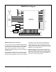
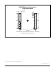
The transceiver module pin-out locations are show in
Figure 2, and the PCB layout for the mating connectors
is shown in Figure 3.
The operating range of the DM2200-916VM critically
depends on the antenna being located properly. When
using the standard DM2200-916VM antenna (RFM part
number 400-1687-001), care should be taken to keep
the antenna at least 0.5 inch away from the sides of its
enclosure. The enclosure must be made from a plastic
with low RF attenuation, such as fiberglass, PVC or
ABS. Note: other antenna configurations are possible,
but each new antenna configuration must be added to
the DM2200-916VM FCC module certification before
deployment. Contact RFM for details.
The DM2200-916VM enclosure should be mounted so
the antenna is at least 4 feet off the ground, and ideally
6 or more feet off the ground.
The DM2200-916VM has an on-board regulator input
on Pin J1-2. To use the on-board regulator, connect
J1-3 to J1-2 and apply a voltage to this connection of at
least 3.1 Vdc, but not greater than 14 Vdc, including rip
-
ple variations. When running from the on-board regula
-
tor, up to 5 mA is available on J1-4 to operate external
circuitry. Any external circuitry connected to J1-4 must
not induce more that 10 mV
P-P
ripple on the regulated
3 Vdc at this pin.
The DM2200-916VM can also be run from an off-board
regulated supply or a battery. In this case, connect J1-3
to ground, leave J1-2 unconnected, and apply the regu-
lated supply or battery input to J1-4. Note the input volt-
age range for J1-4 must be in the range of 2.9 to 3.7
Vdc, with no more than 10 mV
P-P
ripple.
Only pins J1-2 and J1-3 are rated to operate from a
supply voltage higher than 3.7 Vdc. Further, care must
be taken so that analog or logic inputs applied to the
transceiver module stay within the voltage range of 0 to
VDD (voltage at J1-4). Applying a voltage outside of the
0 to VDD voltage range to an analog or logic input can
damage the module.
The DM2200-916VM has current limiting protection re
-
sistors on most of the I/O pins. These limit the current
that a logic output can source or sink. Any DM2200-
915.50SN pin defined as an output should be used only
to drive a high impedance load such as a CMOS logic
input or a MOSFET transistor.
3