
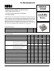
Data Sheet
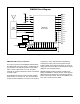


Pin Name Description
J1-1 GND This pin is connected to ground.
J1-2 VIN
This pin is the input to the DM2200-916VM on-board voltage regulator. The minimum input voltage to this pin is
3.1 V, and the maximum input to this pin is 14.0 V.
J1-3 VREN
This pin is the enable input for the DM2200-916VM on-board regulator. To enable the on-board regulator, con
-
nect this pin to J1-2. To disable the on-board regulator, connect this pin to ground.
J1-4 VDD
This pin is connected to the DM2200-916VM positive power supply buss. When the module is powered from
the on-board regulator, this pin can provide up to 5 mA of current at 3.0 Vdc. Note this current adds to the re
-
ceive, transmit and sleep currents listed in the specifications on Page 1. The external load must not impress
more than 10 mV peak -peak ripple on the supply buss. If the on-board regulator is disabled, the module can be
powered through this pin by an external 2.9 to 3.7 Vdc source (maximum ripple 10 mV peak-peak).
J1-5 TD0 This pin is only used for factory programming. It must be left unconnected in normal operation.
J1-6 TDI This pin is only used for factory programming. It must be left unconnected in normal operation.
J1-7 TWS This pin is only used for factory programming. It must be left unconnected in normal operation.
J1-8 TCK This pin is only used for factory programming. It must be left unconnected in normal operation.
J1-9 RST This pin is only used for factory programming. It must be left unconnected in normal operation.
J1-10 CFG0
This pin is a hardware configuration input, reserved for future use. Connect it to J1-4 (positive supply buss) for
normal operation.
J1-11 CFG1
This pin is a hardware configuration input, reserved for future use. Connect it to J1-4 (positive supply buss) for
normal operation.
J1-12 CFG2
This pin is a hardware configuration input, reserved for future use. Connect it to J1-4 (positive supply buss) for
normal operation.
J1-13 CFG3
This pin is a hardware configuration input, reserved for future use. Connect it to J1-4 (positive supply buss) for
normal operation.
J1-14 GND This pin is connected to ground.
J2-1 GND This pin is connected to ground.
J2-2 RXD This pin is the serial data input (CMOS).
J2-3 TXD This pin is the serial data output (CMOS).
J2-4 CTS This pin is a serial data flow control input (CMOS). Hardware flow control is required.
J2-5 RTS This pin is a serial data flow control output (CMOS). Hardware flow control is required.
J2-6 GP0/RSSI
This pin is an I/O pin dedicated to monitoring the RSSI circuit output. It is configured as an analog-to-digital
converter input. The RSSI signal can also be monitored externally at this pin.
J2-7 GP1
This pin is an I/O pin. The default configuration of this pin is a digital input with optional pulse counting capabil
-
ity. A 24-bit register is maintained within the DM2200 to accumulate pulse counts. This input can count up to
10 pulses/second. This input supports interrupts, allowing pulse counting or alarm monitoring while the DM2200
is operating in a low current “sleep” mode.
J2-8 GP2
This pin is an I/O pin. The default configuration of this pin is a digital input. This input supports interrupts, allow
-
ing alarm monitoring while the DM2200 is operating in a low current “sleep” mode.
J2-9 GP3 This pin is an I/O pin. The default configuration of this pin is a digital input.
J2-10 GP4 This pin is an I/O pin. The default configuration of this pin is a digital output.
J2-11 GP5 This pin is an I/O pin. The default configuration of this pin is a digital output.
J2-12 GP6 This pin is an I/O pin. The default configuration of this pin is an analog-to-digital converter input.
J2-13 GP7 This pin is an I/O pin. The default configuration of this pin is an analog-to-digital converter input.
J2-14 GND This pin is connected to ground.
4
Pin Descriptions