
User's Manual


Preliminary Specification Number : SP-ABZ-F
8 / 19
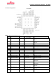
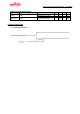
44
GND
Ground
-
-
45
PH1-OSC_OUT
I/O
STM32L082_PH1
GPIO Mode:PH1
High-speed external clock OSC output
46
PH0-OSC_IN
I/O
STM32L082_PH0
GPIO Mode:PH0
High-speed external clock OSC input
47
TCXO_OUT
O
-
Internal TCXO output
48
VDD _TCXO
Power
-
Power supply for the TCXO IC
49~57
GND
Ground
-
Ground
Note: GPIO pins are to be left OPEN if not used.
5. Label Information
TBD
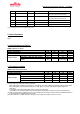
6. Absolute Maximum Ratings
Table 3 Maximum ratings
Parameters
Min
Typ
Max
Unit
Storage Temperature
-40
25
+90
degC
Input RF Level
-
-
10
dBm
Supply Voltage
VDD_USB
-0.3
-
3.9
V
VDD_MCU, VDD_RF, VDD_TCXO
-0.3
-
3.9
V
VREF+
-0.3
-
V
DD_MCU
+0.4
V
7. Operating Condition
Table 4 Operating specification
Parameters
Min
Typ
Max
Unit
Operating Temperature
-40
25
+85
degC
Supply Voltage
VDD_USB (USB peripheral used)
(1)
3.0
-
3.6
V
VDD_USB(USB peripheral not used)
(1)
V
DD_MCU_min
V
DD_MCU
V
DD_MCU_max
V
VDD_MCU,VDD_RF,VDD_TCXO
2.2
(3)
-
3.6
V
VREF+
(2)
1.8
-
VDD_MCU
V
(1) VDD_USB must respect the following conditions:
- When VDD_MCU is powered on (VDD_MCU < VDD_MCU_min), VDD_USB should be always lower than VDD_MCU.
- When VDD_MCU is powered down (VDD_MCU < VDD_MCU_min), VDD_USB should be always lower than
VDD_MCU.
- In operating mode, VDD_USB could be lower or higher than VDD_MCU.
- If the USB is not used, VDD_USB must be tied to VDD_MCU to be able to use PA11 and PA12 as standard I/Os.
(2) VREF+ is used to ensure a better accuracy on low-voltage inputs and outputs of ADC and DAC. Detailed information is
on the STM32L082*** datasheet and user guider.
(3) When module is on +20dBm operation, the supply of the voltage should be set from 2.4V to 3.6V.