
User's Manual


Preliminary Specification Number : SP-1SJ-295
2 / 25
Preliminary & Confidential
< Specification may be changed by Murata without notice >
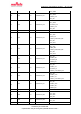
TABLE OF CONTENTS
1.
Features ···················································································································· 3
2.
Part Number ·············································································································· 3
3.
Block Diagram ············································································································ 3
4.
Certification info ········································································································· 3
4.1.
Radio Certification ································································································ 3
5.
Dimensions, Marking and Terminal Configurations ························································· 4
6.
Label Information ······································································································· 9
7.
Absolute Maximum Ratings ·························································································· 9
8.
Operating Condition ···································································································· 9
9.
Electrical Characteristics ···························································································· 10
9.1.
FSK Transceiver Specification ··············································································· 10
9.2.
LoRa Transceiver Specification ·············································································· 10
9.3.
Low power mode current ······················································································· 11
10.
Power Sequences ········································································································ 11
11.
Recommend Land Pattern ··························································································· 12
12.
Reference Circuit ······································································································· 13
13.
Tape and Reel Packing ································································································ 14
13.1.
Dimension of Tape ···························································································· 14
13.2.
Dimensions of Reel ···························································································· 14
13.3.
Taping Diagrams ······························································································ 15
13.4.
Leader and Tail Tape ························································································· 15
14.
Notice ······················································································································· 17
14.1.
Storage Conditions ···························································································· 17
14.2.
Handling Conditions ························································································· 17
14.3.
Standard PCB Design (Land Pattern and Dimensions) ··········································· 17
14.4.
Notice for Chip Placer : ······················································································ 17
14.5.
Soldering Conditions: ······················································································ 17
14.6.
Cleaning : ········································································································ 18
14.7.
Operational Environment Conditions : ································································· 18
14.8.
Input Power Capacity : ······················································································ 18
15.
Regulatory Statements ······························································································· 19