
Datasheet

3. Mounting Instructions
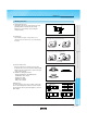
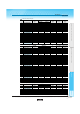
(2) PCB Warping
PCB should be designed so that products are not
subjected to the mechanical stress caused by warping
the board.
Poor example
Products should be located in the sideways direction
(Length: a<b) to the mechanical stress.
Good example
a
b
Poor example
The electrode part of the product should be located
like the picture to the mechanical stress.
Good example
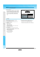
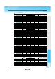
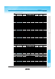
(1) Land Pattern Dimensions
Large lands reduce Q of the mounted chip. Also, large
protruding land areas (bordered by lines having
dimensions 'c' and 'd' shown) cause floating and
electrode leaching.
d
c
Land
Solder Resist
electrode
electrode
LQP/LQG
LQW_H
LQW_A/21H
(3) Amount of Solder Paste
Excessive solder causes electrode corrosion, while
insufficient solder causes low electrode bonding strength.
Adjust the amount of solder paste as shown on the right
so that solder is applied.
" Guideline of solder paste thickness
· LQP (Except LQP02T), LQG, LQW15A/18A/
21H/2BA/2UA: 100 to 150µm
· LQP02T: 50 to 80µm
· LQW04A: 80 to 100µm
· LQW_H: 200 to 300µm
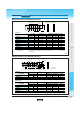
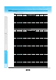
LQW15A Series:
Too much solder may cause slant or rotation of chip at the
time of solder melting. Please reduce the amount of solder
by using smaller solder area than land pattern, as shown in
figure at right.
a
0.65
(in mm)
b
0.35
c
0.50
d
0.30
1.2
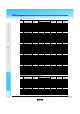
Stencil Pattern
Land Pattern
Solder Resist
a
b
b
c
d
1.2
Stencil Pattern
b
b
c
d
1.2
Land Pattern
a
b
b
c
Continued on the following page.
RF Inductor Soldering and Mounting
169
Inductor for Low Frequency CircuitsRF Inductor
Soldering
and Mounting
Inductor for Power Lines (Power Inductor)
!Note
• Please read rating and !CAUTION (for storage, operating, rating, soldering, mounting and handling) in this catalog to prevent smoking and/or burning, etc.
• This catalog has only typical specifications because there is no space for detailed specifications. Therefore, please review our product specifications or consult the approval sheet for product specifications before ordering.
O05E.pdf
Oct.13,2011