
User's Manual

Chapter 2 Configuration and Installation
© National Instruments Corporation 2-23 Lab-NB User Manual
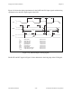
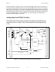
+5 V
I/O Connector
CLK
GATE
OUT
DGND
Lab-NB Board
Gate
Source
Signal
Source
Counter
4.7 kΩ
13
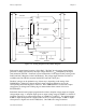
Figure 2-17. Frequency Measurement Application
The GATE, CLK, and OUT signals for counters B1 and B2 are available at the I/O connector. In
addition, the GATE and CLK pins are pulled up to +5 V through a 4.7 kΩ resistor. The input
and output ratings and timing specifications for the 8253 signals are given next.
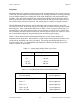
The following specifications and ratings apply to the 8253 I/O signals:
Absolute maximum voltage input rating -0.5 to 7.0 V with respect to DGND
8253 digital input specifications (referenced to DGND):
V
IH
input logic high voltage 2.2 V min
V
IL
input logic low voltage 0.8 V max
Input load current ±10 µA max
8253 digital output specifications (referenced to DGND):
V
OH
output logic high voltage 2.4 V min
V
OL
output logic low voltage 0.45 V max
I
OH
output source current, at V
OH
400 µA max
I
OL
output sink current, at V
OL
2.2 mA max