
User's Manual

Register-Level Programming Chapter 4
Lab-NB User Manual 4-2 © National Instruments Corporation
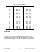
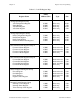
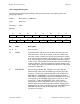
Table 4-1. Macintosh Slot Addresses
Slot Number Starting Address (Hex) Ending Address (Hex)
24-Bit Mode
9 0090 0000 009F FFFF
A 00A0 0000 00AF FFFF
B 00B0 0000 00BF FFFF
C 00C0 0000 00CF FFFF
D 00D0 0000 00DF FFFF
E 00E0 0000 00EF FFFF
32-Bit Mode
0 F000 0000 F0FF FFFF
1 F100 0000 F1FF FFFF
2 F200 0000 F2FF FFFF
3 F300 0000 F3FF FFFF
4 F400 0000 F4FF FFFF
5 F500 0000 F5FF FFFF
6 F600 0000 F6FF FFFF
7 F700 0000 F7FF FFFF
8 F800 0000 F8FF FFFF
9 F900 0000 F9FF FFFF
A FA00 0000 FAFF FFFF
B FB00 0000 FBFF FFFF
C FC00 0000 FCFF FFFF
D FD00 0000 FDFF FFFF
E FE00 0000 FEFF FFFF
Register Map
The register map for the Lab-NB is given in Table 4-2. This table gives the register name, the
register address offset from the board’s base address, the type of the register (read only, write
only, or read and write), and the size of the register in bits.
The register addresses in Table 4-2 are the offset addresses from the slot starting address. To
calculate the absolute address of the register, add the slot starting address given in Table 4-1 to
the register offset given in Table 4-2. For example, if the Lab-NB is plugged into the third slot
(corresponding to slot starting address B0 0000), the ADC FIFO memory is at address B0 0000 +
0 8010, that is, address B0 8010.