
User's Manual
Chapter 4 Register-Level Programming
© National Instruments Corporation 4-39 Lab-NB User Manual
Clearing the Analog Input Circuitry
The analog input circuitry can be cleared by writing to the A/D Clear Register, which leaves the
analog input circuitry in the following state:
• Analog input error flags OVERFLOW and OVERRUN are cleared.
• Pending interrupt requests are cleared.
• A/D FIFO has one garbage word of data.
Empty the A/D FIFO before starting any A/D conversions by performing a read on the A/D
FIFO Register and ignoring the data read. This operation guarantees that the A/D conversion
results read from the A/D FIFO are the results from the initiated conversions rather than leftover
results from previous conversions.
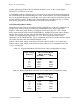
To clear the analog input circuitry and the A/D FIFO, complete these steps:
• Write 0 to the A/D Clear Register (8-bit write).
• Read the A/D FIFO Register and ignore the data (16-bit read).
Programming Multiple A/D Conversions on a Single Input Channel
A sequence of timed A/D conversions is referred to in this manual as a DAQ operation. Two
types of DAQ operations are available on the Lab-NB:
• Controlled acquisition mode
• Freerun acquisition mode
In controlled acquisition mode, two counters (counters A0 and A1) are required for a DAQ
operation. Counter A0 is used as a sample-interval counter, while counter A1 is used as a
sample counter. In this mode, a specified number of conversions is performed, after which the
hardware shuts off the conversions. Counter A0 generates the conversion pulses, and counter A1
gates off counter A0 after the programmed count has expired. The number of conversions in a
single DAQ operation in this case is limited to a 16-bit count (or 65,535).
In freerun acquisition mode, only one counter is required for a DAQ operation. Counter A0
continuously generates the conversion pulses as long as GATEA0 is held at a high logic level.
The software keeps track of the number of conversions that has occurred and turns off counter
A0 after the required number of conversions has been obtained. The number of conversions in a
single DAQ operation in this case is unlimited. Counter A0 is clocked by a 1-MHz clock on start
up.
Alternatively, a programmable timebase for counter A0 is available through the use of counter
B0. If the TBSEL bit in the ADC Configuration Register is set, then the timebase for counter A0
is counter B0. Counter B0 has a fixed, unalterable 2-MHz clock as its own timebase, so its
period is the value stored in it multiplied by 500 nsec. The minimum period that can be selected
for counter B0 is 1 µsec. The period of counter A0, or the sample period, is then equal to the
period of counter B0 multiplied by the value stored in counter A0. Regardless of the timebase
chosen, the minimum sample period of 16 µsec must be observed for data integrity.