
User's Manual

NI PXI/PCI-5114 Specifications 8 ni.com
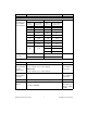
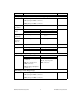
CLK IN (Sample Clock and Reference Clock Input,
Front Panel Connector)
Trigger
Reference (Stop) Trigger
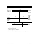
Specification Val ue
Input Voltage Range Sine wave: 0.65 V
pk-pk
to 2.8 V
pk-pk
(0 dBm to 13 dBm)
Square wave: 0.2 V
pk-pk
to 2.8 V
pk-pk
Maximum Input
Overload
7V
rms
with |Peaks| ≤10 V
Impedance 50 Ω
Coupling AC
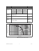
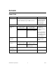
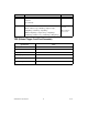
Specification Val ue Comments
Trigger Types
and Sources
Types Sources Refer to the
following
sections and to
NI High-Speed
Digitizers Help
for more
information.
Edge, Window, Hysteresis,
Video, Digital, Immediate,
and Software
CH 0, CH 1, TRIG,
PXI_Trig<0..6>, PFI <0..1>,
PXIStarTrigger,
RTSI<0..6>, and Software
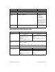
Time
Resolution
TDC Onboard Clock External Clock TDC = Time to
Digital
Conversion
Circuit
On 40 ps N/A
Off 4ns External Clock Period
Rearm Time TDC Rearm Time Holdoff set to 0
On 10 μs
Off 2 μs
Holdoff From Rearm Time up to [(2
35
– 1) × (Sample Clock Period)] —
Trigger Delay From 0 up to [(2
35
– 1) – posttrigger samples] ×
(1/sample rate), in seconds
—