NI 5422 Specifications NI PXI-5422 16-Bit 200 MS/s Arbitrary Waveform Generator Unless otherwise noted, the following conditions were used for each specification: • Analog Filter enabled. • Signals terminated with 50 Ω. • Direct Path set to 1 Vpk-pk, Low-Gain Amplifier Path set to 2 Vpk-pk, and High-Gain Amplifier Path set to 12 Vpk-pk. • Sample rate set to 200 MS/s and the Sample Clock Source set to Divide-by-N.
Environment ............................................................................................32 Safety, Electromagnetic Compatibility, and CE Compliance .................33 Physical....................................................................................................35 Where to Go for Support .........................................................................36 CH 0 (Channel 0 Analog Output, Front Panel Connector) Table 1.
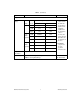
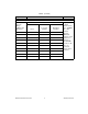
Table 1. (Continued) Specification Value Comments Amplitude and Offset Amplitude Range Amplitude (Vpk-pk) Path Load Minimum Value Maximum Value Direct 50 Ω 0.707 1.00 1 kΩ 1.35 1.91 Open 1.41 2.00 50 Ω 0.00564 2.00 1 kΩ 0.0107 3.81 Open 0.0113 4.00 50 Ω 0.0338 12.0 1 kΩ 0.0644 22.9 Open 0.0676 24.0 LowGain Amplifier HighGain Amplifier Amplitude Resolution 3 digits Offset Range Span of ±50% of Amplitude Range with increments <0.0028% of Amplitude Range.
Table 1. (Continued) Specification Value Comments Maximum Output Voltage Maximum Output Voltage Path Load Maximum Output Voltage (V) Direct 50 Ω ±0.500 1 kΩ ±0.953 Open ±1.000 50 Ω ±1.000 1 kΩ ±1.905 Open ±2.000 50 Ω ±6.000 1 kΩ ±11.43 Open ±12.00 LowGain Amplifier HighGain Amplifier The combination of Amplitude and Offset is limited by the Maximum Output Voltage. Accuracy DC Accuracy For the Low-Gain or High-Gain Amplifier Path: ±0.2% of Amplitude ± 0.
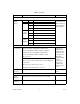
Table 1. (Continued) Specification Value Comments Output Enable Software-selectable. When the Output Path is disabled, the CH 0 Output is terminated to ground with a 1 W resistor equal to the selected output impedance. — Maximum Output Overload The CH 0 output can be connected to a 50 Ω, ±12 V (±8 V for the Direct Path) source without sustaining any damage. No damage occurs if the CH 0 output is shorted to ground indefinitely.
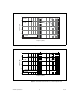
1 +0.4 dB +0.4 dB –0.3 dB –0.3 dB +0.4 dB +0.4 dB Flatness (dB) 0 –1 –1.2 dB –2 –3 Guaranteed Specification Typical –3.4 dB –4 1 10 Frequency (MHz) 100 Figure 1. Normalized Passband Flatness, Direct Path 1 +0.3 dB +0.7 dB +0.7 dB –0.7 dB –0.7 dB +0.7 dB Flatness (dB) 0 –0.5 dB –1 –2 –3 Guaranteed Specification Typical –3.4 dB –4 1 10 Frequency (MHz) 100 Figure 2. Normalized Passband Flatness, Low-Gain Amplifier Path NI 5422 Specifications 6 ni.
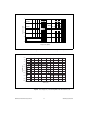
1 +0.2 dB +0.2 dB +0.2 dB –1.1 dB –1.1 dB Flatness (dB) 0 –0.6 dB –1 –2 –3 Guaranteed Specification Typical –4 1 10 Frequency (MHz) 100 Figure 3. Normalized Passband Flatness, High-Gain Amplifier Path 2.0 1.6 1.2 Amplitude (V) 0.8 0.4 0 –0.4 –0.8 –1.2 –1.6 –2.0 0 10 20 30 40 50 60 Time (ns) 70 80 90 100 Figure 4.
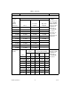
Table 1. (Continued) Specification Value Comments Suggested Maximum Frequencies for Common Functions Function Path Direct Low-Gain Amplifier High-Gain Amplifier 80 MHz 80 MHz 43 MHz Square Not Recommended 50 MHz 25 MHz Ramp Not Recommended 10 MHz 10 MHz Triangle Not Recommended 10 MHz 10 MHz Sine Disable the Analog Filter for square, ramp, and triangle functions.
Table 1. (Continued) Specification Value Comments Path Amplitude –1 dBFS. Measured from DC to 100 MHz. Also called harmonic distortion. SFDR with harmonics at low amplitudes is limited by a –148 dBm/Hz noise floor. All values are typical and include aliased harmonics.
Table 1. (Continued) Specification Value Comments Path Amplitude –1 dBFS. Measured from DC to 100 MHz. SFDR without harmonics at low amplitudes is limited by a –148 dBm/Hz noise floor. All values are typical and include aliased harmonics.
10 0 –10 –20 dBm –30 –40 –50 –60 –70 –80 –90 0 10 20 30 40 50 60 Frequency (MHz) 70 80 90 100 Figure 6. 10 MHz Single-Tone Spectrum, Direct Path, 200 MS/s (Typical) The noise floor in Figure 6 is limited by the measurement device. Refer to the Average Noise Density specification.
10 0 –10 –20 dBm –30 –40 –50 –60 –70 –80 –90 0 10 20 30 40 50 60 Frequency (MHz) 70 80 90 100 Figure 7. 10.00001 MHz Single-Tone Spectrum, Low-Gain Amplifier Path, 200 MS/s (Typical) Note The noise floor in Figure 7 is limited by the measurement device. Refer to the Average Noise Density specification. NI 5422 Specifications 12 ni.
–30 Total Harmonic Distortion (dBc) Guaranteed Specification Typical –40 –44 dBc –49 dBc –50 –60 –67 dBc –70 –80 –90 0.1 1 10 100 Frequency (MHz) Figure 8. Total Harmonic Distortion, Direct Path –30 Total Harmonic Distortion (dBc) Guaranteed Specification Typical –40 –45 dBc –45 dBc –50 –60 dBc –60 –70 –80 –90 0.1 1 10 100 Frequency (MHz) Figure 9.
–30 Total Harmonic Distortion (dBc) Guaranteed Specification Typical –40 –45 dBc –50 –60 –70 –80 –90 0.1 1 10 100 Frequency (MHz) Figure 10. Total Harmonic Distortion, High-Gain Amplifier Path Intermodulation Distortion (dBc) –50 –55 High-Gain –60 –65 Low-Gain –70 –75 Direct Path –80 –85 1 10 Frequency (MHz) 100 Figure 11. Intermodulation Distortion, 200 kHz Separation (Typical) NI 5422 Specifications 14 ni.
10 0 –10 –20 dBm –30 –40 –50 –60 –70 –80 –90 0 10 20 30 40 50 60 Frequency (MHz) 70 80 90 100 Figure 12. Direct Path, Two-Tone Spectrum (Typical) The noise floor in Figure 12 is limited by the noise floor of the measurement device. Refer to the Noise Floor specification. Note Sample Clock Table 2. Specification Sources Value 1. Internal, Divide-by-N (N ≥ 1) 2. Internal, DDS-based, High-Resolution 3. External, CLK IN (SMB front panel connector) 4.
Table 2. (Continued) Specification Value Comments Sample Rate Range and Resolution Sample Clock Source Sample Rate Range Divide-by-N 5 MS/s to 200 MS/s High Resolution — Sample Rate Resolution Settable to (200 MS/s)/N (1 ≤ N ≤ 40) 1.06 µHz 4.24 µHz 5 MS/s to 100 MS/s >100 MS/s to 200 MS/s CLK IN 5 MS/s to 200 MS/s DDC CLK IN 5 MS/s to 200 MS/s PXI Star Trigger 5 MS/s to 105 MS/s PXI_Trig<0..7> 5 MS/s to 20 MS/s Resolution determined by external clock source.
Table 2. (Continued) Specification Value Comments System Phase Noise and Jitter (10 MHz Carrier) Sample Clock Source System Phase Noise Density (dBc/Hz) Offset 100 Hz 1 kHz 10 kHz System Output Jitter (Integrated from 100 Hz to 100 kHz) Divide-by-N –110 –122 –138 1.5 ps rms HighResolution1 100 MS/s –109 –120 –120 4.0 ps rms HighResolution1 200 MS/s –108 –120 –122 4.2 ps rms CLK IN2 –116 –130 –143 1.1 ps rms PXI Star Trigger2,3 –111 –128 –136 2.
Onboard Clock (Internal VCXO) Table 3. Specification Value Comments Clock Source Internal sample clocks can either be locked to a Reference Clock using a phase-locked loop or be derived from the onboard VCXO frequency reference. — Frequency Accuracy ±25 ppm — Phase-Locked Loop (PLL) Reference Clock Table 4. Specification Sources Value 1. PXI_CLK10 (backplane connector) 2.
CLK IN (Sample Clock and Reference Clock Input, Front Panel Connector) Table 5. Specification Value Comments Connector SMB (jack) — Direction Input — Destinations 1. Sample Clock — 2. PLL Reference Clock Frequency Range 5 MHz to 200 MHz (Sample Clock Destination) Input Voltage Range Sine wave: 0.65 Vpk-pk to 2.8 Vpk-pk into 50 Ω (0 dBm to +13 dBm) — 5 MHz to 20 MHz (PLL Reference Clock destination) — Square wave: 0.2 Vpk-pk to 2.
PFI 0 and PFI 1 (Programmable Function Interface, Front Panel Connectors) Table 6. Specification Value Comments Connectors Two SMB (jack) — Direction Bi-directional — Frequency Range DC to 200 MHz — As an Input (Trigger) Destinations Start Trigger — Maximum Input Overload –2 V to +7 V — VIH 2.0 V — VIL 0.8 V — Input Impedance 1 kΩ — As an Output (Event) Sources 1. Sample Clock divided by integer K (1 ≤ K ≤ 4,194,304) — 2.
Table 6. (Continued) Specification Value Comments As an Output (Continued) Maximum Output Overload –2 V to +7 V VOH Minimum: 2.7 V (open load), 1.3 V (50 Ω load) VOL Maximum: 0.6 V (open load), 0.2 V (50 Ω load) Rise/Fall Time (20% to 80%) ≤2.0 ns © National Instruments Corporation — Output drivers are +3.3 V TTL compatible. Measured with a 1 m cable. Load of 10 pF.
DIGITAL DATA & CONTROL (DDC) Optional Front Panel Connector Table 7. Specification Value Comments Connector Type 68-pin VHDCI female receptacle — Number of Data Output Signals 16 — Control Signals 1. DDC CLK OUT (clock output) — 2. DDC CLK IN (clock input) 3. PFI 2 (input) 4. PFI 3 (input) 5. PFI 4 (output) 6. PFI 5 (output) Ground 23 pins — Output Signal Characteristics (Includes Data Outputs, DDC CLK OUT, and PFI<4..
Table 7. (Continued) Specification Value Comments Output Signal Characteristics (Continued) Output Skew Typical: 1 ns, maximum 2 ns. Skew between any two outputs on the DIGITAL DATA & CONTROL front panel connector. — Output Enable/Disable Controlled through the software on all Data Output Signals and Control Signals collectively. When disabled, the outputs go to a high-impedance state. — Maximum Output Overload –0.3 V to +3.9 V — Input Signal Characteristics (Includes DDC CLK IN and PFI<2..
Table 7. (Continued) Specification Value Comments DDC CLK IN Clocking Format DDC Data Output signals change on the rising edge of DDC CLK IN. — Frequency Range 10 Hz to 200 MHz — Input Duty Cycle Tolerance 40% to 60% — Start Trigger Table 8. Specification Sources Value 1. PFI<0..1> (SMB front panel connectors) Comments — 2. PFI<2..3> (DIGITAL DATA & CONTROL front panel connector) 3. PXI_Trig<0..7> (backplane connector) 4. PXI Star trigger (backplane connector) 5.
Table 8. (Continued) Specification Value Comments Delay from Start Trigger to CH 0 Analog Output 65 Sample Clock Periods + 110 ns Refer to ts2 at NI Signal Generators Help»Devices» NI 5422» NI PXI-5422» Triggering» Trigger Timing. Delay from Start Trigger to Digital Data Output 41 Sample Clock periods + 110 ns — Trigger Exporting Exported Trigger Destinations A signal used as a trigger can be routed out to any destination listed in the Destinations specification of Table 9.
Table 9. (Continued) Specification Width Value Comments >150 ns. Refer to tm2 at NI Signal Generators Help» Devices»NI 5422»NI PXI-5422»Waveform Generation» Marker Events. — Skew Destination NI 5422 Specifications With Respect to Digital Data Output PFI<0..1> ±2 Sample Clock Periods N/A PFI<4..5> N/A <2 ns ±2 Sample Clock Periods N/A PXI_Trig<0..
Arbitrary Waveform Generation Mode Table 10. Specification Memory Usage Onboard Memory Size Value Comments The NI 5422 uses the Synchronization and Memory Core (SMC) technology in which waveforms and instructions share onboard memory. Parameters, such as number of segments in sequence list, maximum number of waveforms in memory, and number of samples available for waveform storage, are flexible and user defined.
Table 10. (Continued) Specification Value Comments Loop Count 1 to 16,777,215.
Calibration Table 11. Specification Value Comments Self-Calibration An onboard, 24-bit ADC and precision voltage reference are used to calibrate the DC gain and offset. The self-calibration is initiated by the user through the software and takes approximately 90 seconds to complete. — External Calibration The External Calibration calibrates the VCXO, voltage reference, DC gain, and offset. Appropriate constants are stored in nonvolatile memory.
Power Table 12. Specification Typical Operation Overload Operation Comments 2A 2A +5 VDC Refer to Figure 13 2.7 A +12 VDC 0.46 A 0.46 A –12 VDC 0.01 A 0.01 A 12.2 W + 5 V * 5 V Current 25.7 W Typical Operation is Sine Output, with Analog Filter, 50 Ω termination. 200 MS/s High Resolution Sample Clock. Digital Pattern enabled and terminated, Sample Clock routed to PFI 0 and terminated. +3.3 VDC Total Power Overload Operation occurs when CH 0 is shorted to ground.
Software Table 13. Specification Value Comments Driver Software NI-FGEN version 2.2.1 or later. NI-FGEN is an IVI-compliant driver that allows you to configure, control, and calibrate the NI 5422. NI-FGEN provides application programming interfaces for many development environments.
Environment NI PXI-5422 Environment Note To ensure that the NI PXI-5422 cools effectively, follow the guidelines in the Maintain Forced-Air Cooling Note to Users included in the NI 5422 kit. The NI PXI-5422 is intended for indoor use only. Table 14. Specifications Value Comments Operating Temperature 0 ºC to +55 ºC in all NI PXI chassis except the following: Storage Temperature –25 ºC to +85 ºC. Meets IEC-60068-2-1 and IEC-60068-2-2. — Operating Relative Humidity 10% to 90%, noncondensing.
Safety, Electromagnetic Compatibility, and CE Compliance Table 15. Specification Safety Value Comments The NI 5422 meets the requirements of the following standards of safety for electrical equipment for measurement, control, and laboratory use: For UL and other safety certifications, refer to the product label or to • IEC 61010-1, EN 61010-1 • UL 61010-1 • CAN/CSA-C22.2 No. 61010-1 ni.
Table 15. (Continued) Specification EMC/EMI Value CE, C-Tick, and FCC Part 15 (Class A) Compliant Comments — Notes: 1. This device is not intended for, and is restricted from, use in residential areas. 2. For EMC compliance, operate this device with shielded cabling. 3. When connected to other test objects, this product may cause radio interference. If this occurs, you may be required to take adequate measures to reduce the interference.
Physical Table 16. Specification Value Comments Dimensions 3U, One Slot, PXI/cPCI Module 2.0 × 13.0 × 21.6 cm (0.8 × 5.1 × 8.5 in.) — Weight 352 g (12.4 oz) — Front Panel Connectors Label Function(s) Connector Type CH 0 Analog Output SMB (jack) CLK IN Sample clock input and PLL reference clock input. SMB (jack) PFI 0 Marker output, trigger input, sample clock output, exported trigger output, and PLL reference clock output.
Where to Go for Support The National Instruments Web site is your complete resource for technical support. At ni.com/support you have access to everything from troubleshooting and application development self-help resources to email and phone assistance from NI Application Engineers. A Declaration of Conformity (DoC) is our claim of compliance with the Council of the European Communities using the manufacturer’s declaration of conformity.