
User's Manual

© National Instruments Corporation 2-1 NI PCI-1426 User Manual
2
Hardware Overview
This chapter provides an overview of NI 1426 hardware functionality and
explains the operations of the NI 1426 functional units.
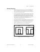
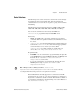
Functional Overview
The NI 1426 features a flexible, high-speed data path optimized for
receiving and formatting video data from Camera Link cameras.
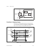
Figure 2-1 illustrates the key functional components of the NI 1426.
Figure 2-1. NI 1426 Block Diagram
Data
MDR 26-Pin Connector
Channel
Link
Receiver
Enables
Pixel
Clock
Camera
Control
UART
PCI Bus
PCI Interface
and
Scatter-Gather
DMA Controllers
Data
SDRAM
Interface
Synchronous Dynamic RAM
Advanced
Timing
Acquisition,
ROI, and Triggering
External Triggers
Pixel Clock and Camera Enables
RTSI Bus
Data
Differential
Converter
15-Pin D-SUB
Serial
Control