NI 5441 Specifications NI PXI-5441 16-Bit 100 MS/s Arbitrary Waveform Generator with Onboard Signal Processing (OSP) Unless otherwise noted, the following conditions were used for each specification: • Analog Filter enabled. • DAC Interpolation set to maximum allowed factor for a given sample rate. • Signals terminated with 50 Ω. • Direct Path set to 1 Vpk-pk, Low-Gain Amplifier Path set to 2 Vpk-pk, and High-Gain Amplifier Path set to 12 Vpk-pk. • Sample clock set to 100 MS/s.
Arbitrary Waveform Generation Mode ...................................................25 Function Generation Mode ......................................................................28 Onboard Signal Processing......................................................................29 Calibration ...............................................................................................38 Power .......................................................................................................
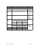
Specification Value Comments Amplitude and Offset Amplitude Range Amplitude (Vpk-pk) Path Load Minimum Value Maximum Value Direct 50 Ω 0.707 1.00 1 kΩ 1.35 1.91 Open 1.41 2.00 50 Ω 0.00564 2.00 1 kΩ 0.0107 3.81 Open 0.0113 4.00 50 Ω 0.0338 12.0 1 kΩ 0.0644 22.9 Open 0.0676 24.0 LowGain Amplifier HighGain Amplifier Amplitude Resolution 3 digits Offset Range Span of ±25% of Amplitude Range with increments <0.0014% of Amplitude Range. 1.
Specification Value Comments Accuracy DC Accuracy For the Low-Gain or High-Gain Amplifier Path: ±0.2% of Amplitude ± 0.05% of Offset ± 500 µV (within ±10 °C of self-calibration temperature) ±0.4% of Amplitude ± 0.05% of Offset ± 1 mV (0 °C to 55 °C) For the Direct Path: Gain Accuracy: ±0.2% (within ±10 °C of self-calibration temperature) All paths are calibrated for amplitude and gain errors. The Low-Gain and High-Gain Amplifier Paths also are calibrated for offset errors. Gain Accuracy: ±0.
Specification Value Comments Frequency and Transient Response Bandwidth 43 MHz Measured at –3 dB. DAC Digital Interpolation Filter Software-selectable Finite Impulse Response (FIR) filter. Available interpolation factors are 2, 4, or 8. Refer to the Onboard Signal Processing section for OSP Interpolation. Analog Filter Software-selectable 7-pole elliptical filter for image suppression. Available only on Low-Gain Amplifier and High-Gain Amplifier Paths.
2.0 1.0 +0.3 dB +0.4 dB –0.4 dB –0.4 dB +0.6 dB 0.0 –1.0 –0.4 dB –2.0 dB –3.0 –4.0 –5.0 –6.0 –7.0 –8.0 Guaranteed Specification Typical –9.0 –10.0 1.0M 10.0M 48.0M Frequency (Hz) Figure 1. Normalized Passband Flatness, Direct Path 2.0 1.6 1.2 Amplitude (V) 0.8 0.4 0.0 –0.4 –0.8 –1.2 –1.6 –2.0 0.0 20.0n 40.0n 60.0n 80.0n 100.0n Time (s) Figure 2. Pulse Response, Low-Gain Amplifier Path 50 Ω Load NI 5441 Specifications 6 ni.
5.0 2.5 0.0 –2.5 –5.0 –7.5 dBm –10.0 –12.5 –15.0 –17.5 –20.0 –22.5 –25.0 –27.5 –30.0 0.0 20.0M 40.0M 60.0M 80.0M 100.0M 120.0M 140.0M 160.0M 180.0M 200.0M Frequency (Hz) Figure 3. Frequency Response of Direct Path, 100 MS/s, 1x DAC Interpolation Note Above 50 MHz, the response is the image response.
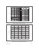
Specification Value Comments Suggested Maximum Frequencies for Common Functions Function Path Direct Low-Gain Amplifier High-Gain Amplifier 43 MHz 43 MHz 43 MHz Square Not recommended* 25 MHz 12.5 MHz Ramp Not recommended* 5 MHz 5 MHz Triangle Not recommended* 5 MHz 5 MHz Sine Disable the Analog Filter and the DAC Interpolation Filter for Square, Ramp, and Triangle. * Direct Path is optimized for the frequency domain.
Specification Value Comments Spurious-Free Dynamic Range (SFDR) with Harmonics Path Amplitude –1 dBFS. Measured from DC to 50 MHz. Also called harmonic distortion. SFDR with harmonics at low amplitudes is limited by a –148 dBm/Hz noise floor. All values are typical and include aliased harmonics.
Specification Value Comments 0 ºC to 40 ºC Total Harmonic Distortion (THD) Path Amplitude –1 dBFS. Includes the 2nd through the 6th harmonic.
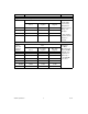
Specification Value Comments Spectral Characteristics (Continued) Average Noise Density Amplitude Range Average Noise Density Path Vpk-pk dBm nV ----------Hz Direct 1 4.0 18 –142 –146.0 Low Gain 0.06 –20.4 9 –148 –127.6 Low Gain 0.1 –16.0 9 –148 –132.0 Low Gain 0.4 –4.0 13 –145 –141.0 Low Gain 1 4.0 18 –142 –146.0 Low Gain 2 10.0 35 –136 –146.0 High Gain 4 16.0 71 –130 –146.0 High Gain 12 25.6 213 –120 –145.
10.0 0.0 –10.0 –20.0 dBm –30.0 –40.0 –50.0 –60.0 –70.0 –80.0 –90.0 0.0 25.0M 50.0M 75.0M 100.0M 125.0M 158.0M 175.0M 200.0M Frequency (Hz) Figure 4. 10 MHz Single-Tone Spectrum, Direct Path, 100 MS/s, DAC Interpolation Factor Set to 4 Note The noise floor in Figure 4 is limited by the measurement device. Refer to the Average Noise Density specifications. NI 5441 Specifications 12 ni.
20.0 10.0 0.0 –10.0 dBm –20.0 –30.0 –40.0 –50.0 –60.0 –70.0 –80.0 –90.0 0.0 25.0M 50.0M 75.0M 100.0M 125.0M 150.0M 175.0M 200.0M Frequency (Hz) Figure 5. 10 MHz Single-Tone Spectrum, Low-Gain Amplifier Path, 100 MS/s, DAC Interpolation Factor Set to 4 The noise floor in Figure 5 is limited by the measurement device. Refer to the Average Noise Density specifications.
10.0 0.0 –10.0 –20.0 dBm –30.0 –40.0 –50.0 –60.0 –70.0 –80.0 –90.0 0.0 25.0M 50.0M 75.0M 100.0M 125.0M 150.0M 175.0M 200.0M Frequency (Hz) Figure 6. Direct Path, 2-Tone Spectrum (Typical) The noise floor in Figure 6 is limited by the measurement device. Refer to the Average Noise Density specifications. Note Sample Clock Specification Sources Value 1. Internal, Divide-by-N (N ≥ 1) 2. Internal, DDS-based, High-Resolution 3. External, CLK IN (SMB front panel connector) 4.
Specification Value Comments Sample Rate Range and Resolution Sample Clock Source Divide-by-N High Resolution CLK IN — Sample Rate Range Sample Rate Resolution 23.84 S/s to 100 MS/s Settable to (100 MS/s) / N (1 ≤ N ≤ 4,194,304) 10 S/s to 100 MS/s 1.06 µHz 200 kS/s to 105 MS/s DDC CLK IN 10 S/s to 105 MS/s PXI Star Trigger 10 S/s to 105 MS/s PXI_Trig<0..7> 10 S/s to 20 MS/s Resolution determined by external clock source. External Sample Clock duty cycle tolerance 40% to 60%.
Specification Value Comments System Phase Noise and Jitter (10 MHz Carrier) Sample Clock Source System Phase Noise Density (dBc/Hz) Offset 100 Hz 1 kHz 10 kHz System Output Jitter (Integrated from 100 Hz to 100 kHz) Divide-by-N –110 –131 –137 <1.0 ps rms HighResolution1 –114 –126 –126 <4.0 ps rms CLK IN –113 –132 –135 <1.1 ps rms PXI Star Trigger2 –115 –118 –130 <3.0 ps rms External Sample Clock Input Jitter Tolerance Cycle-Cycle Jitter ±300 ps 1.
Onboard Clock (Internal VCXO) Specification Value Comments Clock Source Internal sample clocks can either be locked to a Reference Clock using a phase-locked loop or be derived from the onboard VCXO frequency reference. — Frequency Accuracy ±25 ppm — Phase-Locked Loop (PLL) Reference Clock Specification Sources Value 1. PXI_CLK10 (backplane connector) 2. CLK IN (SMB front panel connector) Comments The PLL Reference Clock provides the reference frequency for the PLL.
CLK IN (Sample Clock and Reference Clock Input, Front Panel Connector) Specification Value Comments Connector SMB (jack) — Direction Input — Destinations 1. Sample Clock — 2. PLL Reference Clock Frequency Range 1 MHz to 105 MHz (Sample Clock destination and sine waves) — 200 kHz to 105 MHz (Sample Clock destination and square waves) 5 MHz to 20 MHz (PLL Reference Clock destination) Input Voltage Range Sine wave: 0.65 Vpk-pk to 2.8 Vpk-pk into 50 Ω (0 dBm to +13 dBm) — Square wave: 0.
PFI 0 and PFI 1 (Programmable Function Interface, Front Panel Connectors) Specification Value Comments Connectors Two SMB (jacks) — Direction Bidirectional — Frequency Range DC to 105 MHz — As an Input (Trigger) Destinations Start Trigger — Maximum Input Overload –2 V to +7 V — VIH 2.0 V — VIL 0.8 V — Input Impedance 1 kΩ — As an Output (Event) Sources 1. Sample Clock divided by integer K (1 ≤ K ≤ 4,194,304) — 2.
DIGITAL DATA & CONTROL (DDC) Optional Front Panel Connector Specification Value Comments Connector Type 68-pin VHDCI female receptacle — Number of Data Output Signals 16 — Control Signals 1. DDC CLK OUT (clock output) — 2. DDC CLK IN (clock input) 3. PFI 2 (input) 4. PFI 3 (input) 5. PFI 4 (output) 6. PFI 5 (output) Ground 23 pins — Output Signal Characteristics (Includes Data Outputs, DDC CLK OUT, and PFI<4..
Specification Value Comments Output Signal Characteristics (Continued) Output Skew Typical: 1 ns, maximum 2 ns. Skew between any two outputs on the DIGITAL DATA & CONTROL front panel connector. — Output Enable/Disable Controlled through the software on all Data Output Signals and Control Signals collectively. When disabled, the outputs go to a high-impedance state. — Maximum Output Overload –0.3 V to +3.9 V — Input Signal Characteristics (Includes DDC CLK IN and PFI<2..
Specification Value Comments DDC CLK IN Clocking Format DDC Data Output signals change on the rising edge of DDC CLK IN. — Frequency Range 10 Hz to 105 MHz — Input Duty Cycle Tolerance 40% to 60% — Input Jitter Tolerances 300 ps pk-pk of Cycle-Cycle Jitter, and 1 ns rms of Period Jitter. — Start Trigger Specification Sources Value 1. PFI<0..1> (SMB front panel connectors) Comments — 2. PFI<2..3> (DIGITAL DATA & CONTROL front panel connector) 3. PXI_Trig<0..7> (backplane connector) 4.
Specification Delay from Start Trigger to CH 0 Analog Output with OSP Disabled. Value DAC Interpolation Factor Comments Typical Delay Digital Interpolation Filter disabled. 44 Sample Clock Periods + 110 ns 2 58 Sample Clock Periods + 110 ns 4 64 Sample Clock Periods + 110 ns 8 65 Sample Clock Periods + 110 ns Refer to the ts2 documentation in the NI Signal Generators Help by navigating to NI Signal Generators Help»Devices» NI 5441» Triggering» Trigger Timing.
Markers Specification Destinations Value Comments 1. PFI<0..1> (SMB front panel connectors) — 2. PFI<4..5> (DIGITAL DATA & CONTROL front panel connector) 3. PXI_Trig<0..6> (backplane connector) Quantity One Marker per Segment. — Quantum Marker position must be placed at an integer multiple of four samples (two samples for Complex (IQ) data). — Width >150 ns.
Arbitrary Waveform Generation Mode Specification Value Comments Memory Usage The NI 5441 uses the Synchronization and Memory Core (SMC) technology in which waveforms and instructions share onboard memory. Parameters, such as number of segments in sequence list, maximum number of waveforms in memory, and number of samples available for waveform storage, are flexible and user defined.
Specification Minimum Waveform Size (Samples) Value Comments Trigger Mode Arbitrary Waveform Mode Arbitrary Sequence Mode Single 16 16 Continuous 16 96 @ >50 MS/s 32 @ ≤50 MS/s Stepped 32 96 @ >50 MS/s 32 @ ≤50 MS/s Burst 16 The Minimum Waveform Size is sample rate dependent in Arbitrary Sequence mode. For Complex (IQ) data Minimum Waveform Size is halved. 512 @ >50 MS/s 256 @ ≤50 MS/s Loop Count 1 to 16,777,215.
Specification Value Comments Memory Limits (Continued) Arbitrary Sequence Mode, Maximum Waveforms Arbitrary Sequence Mode, Maximum Segments in a Sequence 262,000 2,097,000 4,194,000 Burst trigger: 32,000 Burst trigger: 262,000 Burst trigger: 524,000 418,000 3,354,000 6,708,000 Burst trigger: 262,000 Burst trigger: 2,090,000 Burst trigger: 4,180,000 Condition: One or two segments in a sequence. Condition: Waveform memory is <4,000 samples. (<2,000 samples for Complex (IQ) Data.
Function Generation Mode Specification Value Standard Waveforms and Maximum Frequencies Memory Size Comments Waveform Maximum Frequency Sine 43 MHz Square 25 MHz Triangle 5 MHz Ramp Up 5 MHz Ramp Down 5 MHz DC — Noise (Pseudo-Random) 5 MHz User Defined 43 MHz 65,536 Samples for 1/4 symmetric waveforms (Example: Sine) 16, 384 Samples for non-1/4 symmetric waveforms (Example: Ramp) — 16-bit samples. User Defined Waveforms must be exactly 16,384 samples.
Onboard Signal Processing Onboard Signal Processing Pre-Filter Gain I Waveform Memory Output Engine Pre-Filter Offset I I FIR I CIC X IQ Rate – Pre-Filter Gain Q Pre-Filter Offset Q Q FIR Q CIC Rate Change (OSP Interpolation) DAC Interpolation DAC X Iφ IQ Rate Digital Gain Qφ NCO Sample Rate Rate Change Effective Sample Rate Figure 7.
Specification Value Comments Pre-Filter Offset Range –1.0 to +1.
Specification Value Comments FIR Filter Types Filter Type Parameter Minimum Maximum — — — Passband 0.1 0.43 Lowpass Filter that minimizes ripple to: IQ Rate × Passband. BT 0.1 0.9 — Raised Cosine Alpha 0.1 0.9 Root Raised Cosine Alpha 0.1 0.9 Custom Flat Gaussian — Coefficients are provided by the user. CIC (Cascaded Integrator-Comb) Filter Size 6 Stages Interpolation Range 6 ≤ Interpolation ≤ 256 (integers) The CIC Filter does the majority of the interpolation in the OSP.
Specification Value Comments Modulation Performance (Typical) Modulation Configuration GSM Physical Layer1 W-CDMA Physical Layer2 DVB Physical Layer3 Measurement Type FIR Interpolation — 2 4 8 MER (Modulation Error Ratio) 46 dB 47 dB 42 dB EVM (Error Vector Magnitude) <0.5 % rms <0.5 % rms <0.8 % rms MER (Modulation Error Ratio) 46 dB 39 dB — EVM (Error Vector Magnitude) <0.5 % rms <1.
Specification Value Comments Digital Performance Maximum NCO Spur FIR Interpolation < –90 dBc IQ Rate Range (with 100 MS/s Sample Clock Rate) Full-Scale Output — OSP Out of Band Suppression OSP Passband Ripple 2 195 kS/s to 8.33 MS/s 63 dB 0 to –0.08 dB 4 97.6 kS/s to 4.16 MS/s 74 dB 0 to –0.08 dB 8 48.8 kS/s to 2.08 MS/s 40 dB 0 to –0.8 dB © National Instruments Corporation 33 FIR Filter Type = Flat. Passband = 0.4. Ripple Measurement to 0.4 × IQ Rate. Stop Band Suppression from 0.
Figure 8. GSM Physical Layer1 External Sample Clocking = 99.665 MHz Figure 9. GSM Physical Layer1 Internal (High Resolution) Sample Clocking = 99.665 MHz Additional artifacts are due to High Resolution Clock spurs. 1 OSP Enabled. Direct Path (4 dBm Peak). 25 MHz Carrier. IQ Rate = 1.083 MS/s, 4 Samples/Symbol. FIR Filter Type = Flat, Passband = 0.4. Software MSK modulation: 270.833 kS/s, Gaussian, BT = 0.3. PN Sequence Order = 14. NI 5441 Specifications 34 ni.
Figure 10. CDMA 2000 Physical Layer1 External Sample Clocking = 98.304 MHz Figure 11. CDMA 2000 Physical Layer1 Internal (High Resolution) Sample Clocking = 98.304 MHz Additional artifacts are due to High Resolution Clock spurs. 1 OSP Enabled. Direct Path (4 dBm Peak). 25 MHz Carrier. IQ Rate = 1.2288 MS/s, 1 Sample/Symbol. FIR Filter Type = Custom Flat Filter with Passband = 0.48. QPSK. PN Sequence Order = 15.
Figure 12. W-CDMA Physical Layer1 External Sample Clocking = 92.16 MHz Figure 13. W-CDMA Physical Layer1 Internal (High Resolution) Sample Clocking = 92.16 MHz Additional artifacts are due to High Resolution Clock spurs. 1 OSP Enabled. Direct Path (4 dBm Peak). 25 MHz Carrier. IQ Rate = 3.84 MS/s, 1 Sample/Symbol. FIR Filter Type = Root Raised Cosine, Alpha = 0.22. QPSK. PN Sequence Order = 15. NI 5441 Specifications 36 ni.
Figure 14. DVB Physical Layer1 External Sample Clocking = 96.88 MHz Artifacts at 15 and 35 MHz are due to 2x FIR Interpolation aliasing. Figure 15. DVB Physical Layer1 Internal (High Resolution) Sample Clocking = 96.88 MHz Artifact at 10 MHz is due to CLK IN feed-through. Additional artifacts are due to High Resolution Clock spurs. 1 OSP Enabled. Direct Path (4 dBm Peak). 25 MHz Carrier. IQ Rate = 6.92 MS/s, 1 Sample/Symbol. FIR Filter Type = Root Raised Cosine, Alpha = 0.15. 32 QAM Modulation.
Calibration Specification Value Comments Self-Calibration An onboard, 24-bit ADC and precision voltage reference are used to calibrate the DC gain and offset. The self-calibration is initiated by the user through the software and takes approximately 75 seconds to complete. — External Calibration The External Calibration calibrates the VCXO, voltage reference, output impedance, DC gain, and offset. Appropriate constants are stored in nonvolatile memory.
Software Specification Value Comments Driver Software NI-FGEN 2.3 or later version. NI-FGEN is an IVI-compliant driver that allows you to configure, control, and calibrate the NI 5441. NI-FGEN provides application programming interfaces for many development environments. — Application Software NI-FGEN provides programming interfaces for the following application development environments: — • LabVIEW • LabWindows™/CVI™ • Measurement Studio • Microsoft Visual C++ .
Environment NI PXI-5441 Environment Note To ensure that the NI PXI-5441 cools effectively, follow the guidelines in the Maintain Forced-Air Cooling Note to Users included in the NI 5441 kit. The NI PXI-5441 is intended for indoor use only. Specifications Operating Temperature Value 0 ºC to +55 ºC in all NI PXI chassis except the following: Comments — 0 ºC to +45 ºC when installed in an NI PXI-101x or NI PXI-1000B chassis. Meets IEC-60068-2-1 and IEC-60068-2-2. Storage Temperature –25 ºC to +85 ºC.
Safety, Electromagnetic Compatibility, and CE Compliance Specification Safety Value Comments The NI 5441 meets the requirements of the following standards of safety for electrical equipment for measurement, control, and laboratory use: For UL and other safety certifications, refer to the product label or visit • IEC 61010-1, EN 61010-1 ni.com/ certification. • UL 61010-1 • CAN/CSA-C22.2 No.
Physical Specification Value Comments Dimensions 3U, One Slot, PXI/cPCI Module 2.0 × 13.0 × 21.6 cm (0.8 × 5.1 × 8.5 in) — Weight 345 g (12.1 oz) — Front Panel Connectors Label Function(s) Connector Type CH 0 Analog Output SMB (jack) CLK IN Sample clock input and PLL reference clock input. SMB (jack) PFI 0 Marker output, trigger input, sample clock output, exported trigger output, and PLL reference clock output.
Technical Support Resources NI Web Support National Instruments Web support is your first stop for help in solving installation, configuration, and application problems and questions. Online problem-solving and diagnostic resources include frequently asked questions, knowledge bases, product-specific troubleshooting wizards, manuals, drivers, software updates, and more. Web support is available through the Technical Support section of ni.com.
National Instruments, NI, ni.com, and LabVIEW are trademarks of National Instruments Corporation. Refer to the Terms of Use section on ni.com/legal for more information about National Instruments trademarks. Other product and company names mentioned herein are trademarks or trade names of their respective companies. For patents covering National Instruments products, refer to the appropriate location: Help»Patents in your software, the patents.txt file on your CD, or ni.com/patents.