VXI-SC-1102/B/C User Manual 32-Channel Multiplexer Amplifier Submodules August 1997 Edition Part Number 321385B-01 © Copyright 1997 National Instruments Corporation. All rights reserved.
Internet Support support@natinst.com E-mail: info@natinst.com FTP Site: ftp.natinst.com Web Address: http://www.natinst.com Bulletin Board Support BBS United States: (512) 794-5422 BBS United Kingdom: 01635 551422 BBS France: 01 48 65 15 59 Fax-on-Demand Support (512) 418-1111 Telephone Support (U.S.
Important Information Warranty The VXI-SC-1102,VXI-SC-1102B, and VXI-SC-1102C submodules are warranted against defects in materials and workmanship for a period of one year from the date of shipment, as evidenced by receipts or other documentation. National Instruments will, at its option, repair or replace equipment that proves to be defective during the warranty period. This warranty includes parts and labor.
Table of Contents About This Manual Organization of This Manual ........................................................................................ ix Conventions Used in This Manual................................................................................ x National Instruments Documentation ........................................................................... xi Related Documentation.................................................................................................
Table of Contents Chapter 4 Theory of Operation Functional Overview .................................................................................................... 4-1 VXIbus Interface .......................................................................................................... 4-2 Digital Control Circuitry .............................................................................................. 4-2 Analog Circuitry.....................................................................
Table of Contents Figure 3-1. Figure 3-2. Figure 3-3. VXI-SC-1102/B/C Front Connector Pin Assignments.......................... 3-2 Ground-Referenced Signal Connection ................................................. 3-5 Floating Signal Connection Referenced to Chassis Ground.................. 3-6 Figure 4-1. VXI-SC-1102/B/C Block Diagram........................................................ 4-1 Figure 5-1. Analog Bus Receptacle Pin Assignment ...............................................
About This Manual This manual describes the electrical and mechanical aspects of the VXI-SC-1102 family and contains information concerning their installation and operation. The VXI-SC-1102 family is a group of signal conditioning submodules in the VXI-data acquisition (VXI-DAQ) line of National Instruments products.
About This Manual • Chapter 4, Theory of Operation, contains a functional overview of the VXI-SC-1102/B/C submodules and explains the operation of each functional unit. • Chapter 5, Calibration, discusses the calibration procedures for the VXI-SC-1102/B/C submodules. • Appendix A, Specifications, lists the specifications for the VXI-SC-1102/B/C submodules. • Appendix B, Calibration Sample Program, contains a sample program to help you calibrate your submodule.
About This Manual examples. This font is also used for the proper names of disk drives, paths, directories, programs, subprograms, subroutines, device names, functions, variables, file names, and extensions, and for statements and comments taken from program code. carrier module Refers to the VXI-SC-1000, which plugs directly into a VXI slot and on which VXI-SC submodules are installed. PC Refers to the IBM PC/XT, the IBM PC AT, and compatible computers.
About This Manual • Accessory installation guides or manuals—If you are using accessory products, read the terminal block and cable assembly installation guides or accessory device user manuals. They explain how to physically connect the relevant pieces of the system. Consult these guides when you are making your connections.
Chapter 1 Introduction This chapter describes the VXI-SC-1102 family of submodules; lists what you need to get started, optional software, and optional equipment; and explains how to unpack your VXI-SC-1102/B/C submodule. The VXI-SC-1102 family is part of the VXI signal conditioning system, which consists of a carrier module and one or more VXI signal conditioning submodules or filler panels as shown in Figure 1-1.
Chapter 1 Introduction The VXI-SC-1000 is a carrier module that installs into a slot in a VXIbus chassis and is populated with one or two submodules. The VXI-SC-1102/B/C is a submodule that installs into VXI-SC subslots on a VXI-SC-1000 carrier module. Your VXI-SC-1000 carrier module is shipped with a filler panel installed in one of the submodule sites. This filler panel is necessary for the attachment of the front panel, so you should leave it in place until you are ready to install a VXI-SC submodule.
Chapter 1 Introduction The VXI-SC-1102/B/C submodules operate with full functionality with National Instruments VXI-MIO modules. You can multiplex several VXI-SC-1102/B/C submodules and other VXI signal conditioning submodules into a single channel on the VXI-MIO module, greatly increasing the number of analog input signals that you can digitize. You can also use National Instruments terminal blocks, which have screw terminals to which you attach the input signals for the VXI-SC-1102/B/C submodules.
Chapter 1 Introduction Software Programming Choices There are several options to choose from when programming your National Instruments VXI-DAQ hardware. You can use LabVIEW, LabWindows/CVI, ComponentWorks, VirtualBench, or other application development environments with either NI-DAQ or the VXIplug&play instrument driver. Both NI-DAQ and the VXIplug&play instrument driver access the VXI-DAQ hardware through the VISA driver software.
Chapter 1 Introduction NI-DAQ Driver Software The NI-DAQ driver software is included at no charge with all National Instruments DAQ hardware. NI-DAQ is not packaged with accessory products. NI-DAQ has an extensive library of functions that you can call from your application programming environment.
Chapter 1 Introduction VXIplug&play Instrument Driver National Instruments distributes VXIplug&play instrument drivers free of charge. VXIplug&play instrument drivers are one level above the NI-DAQ device driver and contain high-level software functions whose architecture is specified by the VXIplug&play Systems Alliance. The VXIplug&play standards increase interoperability with other vendors, and ensure that drivers are designed and presented in a consistent fashion that facilitates ease of use.
Chapter 1 Introduction Unpacking Your VXI-SC-1102/B/C submodule is shipped in an antistatic package to prevent electrostatic damage to the submodule. Electrostatic discharge can damage several components on the submodule. To avoid such damage in handling the submodule, take the following precautions: • Ground yourself via a grounding strap or by holding a grounded object. • Touch the antistatic package to a metal part of your VXIbus chassis before removing the submodule from the package.
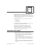
Chapter 2 Installation This chapter describes how to install current-loop receivers on your VXI-SC-1102/B/C and gives information about installing your VXI-SC-1102/B/C into the VXI-SC-1000 carrier module. Refer to Figure 2-1, VXI-SC-1102/B/C Parts Locator Diagram, for information as you read the instructions in this chapter.
Chapter 2 Installation 2 3 1 4 1 Serial Number 2 Product Name 3 Assembly Number 4 RCLx Pads Figure 2-1.
Chapter 2 Installation Current-Loop Receivers The VXI-SC-1102/B/C submodules have pads for transforming individual channels to current-to-voltage converters. National Instruments offers an SCXI Process Current Resistor Kit of four 249 Ω, 0.1%, 5 ppm, 1/4 W resistors. The reference designators for the current loop resistors have the following format: for input channel x, the resistor is RCLx. For example, the resistor for channel 28 is RCL28.
Chapter 2 Installation Installing Your Hardware Follow the instructions in the VXI-SC-1000 Carrier Module Installation Guide to install the assembled VXI-SC carrier module in the VXIbus chassis.
Chapter 3 Signal Connections This chapter describes the analog input signal connections to the VXI-SC-1102/B/C submodule via the front connector. ! Caution: Static electricity is a major cause of component failure. To prevent damage to the electrical components in the module, observe antistatic techniques whenever removing a module from the chassis or whenever working on a module. Front Connector Figure 3-1 shows the pin assignments for the VXI-SC-1102/B/C submodule front connector.
Chapter 3 Signal Connections A CGND NC NC NC NC NC NC NC CGND NC NC NC NC NC NC NC CGND NC NC NC NC NC NC NC NC NC NC CGND CJSENSOR CJSENSOR CGND +5 V B 32 31 30 29 28 27 26 25 24 23 22 21 20 19 18 17 16 15 14 13 12 11 10 9 8 7 6 5 4 3 2 1 CH0CH1CH2CH3CH4CH5CH6CH7CH8CH9CH10CH11CH12CH13CH14CH15CH16CH17CH18CH19CH20CH21CH22CH23CH24CH25CH26CH27CH28CH29CH30CH31- 32 31 30 29 28 27 26 25 24 23 22 21 20 19 18 17 16 15 14 13 12 11 10 9 8 7 6 5 4 3 2 1 C CH0+ CH1+ CH2+ CH3+ CH4+ CH5+ CH6+ CH7+ CH8+ CH9+ CH10+
Chapter 3 Signal Connections Signal Descriptions Table 3-1. Front Connector Signal Descriptions Pin Signal Name Description A1 +5 V +5 VDC Source—Powers the temperature sensor on the terminal block. 0.2 mA of source not protected. A2, A5, A16, A24, A32 CGND Chassis Ground—Tied to the VXIbus chassis. A3, A4 CJSENSOR Cold-Junction Temperature Sensor Input—Connects to the temperature sensor of the terminal block.
Chapter 3 Signal Connections channel is ±11 V. This common-mode input range for either positive or negative channel input is the maximum input voltage (relative to CGND) that will result in a valid measurement. Each channel includes input protection circuitry to withstand the accidental application of voltages up to ±42 VAC peak or VDC.
Chapter 3 CH0 + Signal Connections + CH0 + Vdiff CH1 + + CH1 Vcm - Front Signal Connector + VXI-SC-1102/B/C Figure 3-2.
Chapter 3 Signal Connections CH0 + + CH0 Floating Signal + Vs CH1 + + CH1 - Front Signal Connector - Make this connection to ground reference the signal. CGND Reference to Chassis Ground VXI-SC-1102/B/C Figure 3-3. Floating Signal Connection Referenced to Chassis Ground Cold-Junction Sensor Connection Pins A3 and A4 (CJSENSOR) connect the temperature sensor located on the National Instruments VXI-TB Series terminal block to the VXI-SC-1102/B/C. The CJSENSOR signal is measured relative to CGND.
Chapter 4 Theory of Operation This chapter contains a functional overview of the VXI-SC-1102/B/C submodules and explains the operation of each functional unit. Functional Overview CH 0 – + Inst. Amp Lowpass Filter Buffer Lowpass Filter Buffer Buffer Mux CH 0 + Input Protection and Lowpass Filter The block diagram in Figure 4-1 illustrates the key functional components of the VXI-SC-1102/B/C submodules. – 32-to-1 Mux CH 31 – + Inst.
Chapter 4 Theory of Operation The major components of the VXI-SC-1102/B/C submodules are as follows: • VXIbus interface • Digital control circuitry • Analog circuitry The VXI-SC-1102/B/C submodules consist of 32 multiplexed input channels, each with a software-programmable gain of 1 or 100. Each input channel has its own lowpass filter. The VXI-SC-1102/B/C submodules also have digital control circuitry for automatic control of channel scanning, temperature sensor selection, and gain selection.
Chapter 4 Theory of Operation Introduction, of this manual to learn about options for programming the control circuitry. Analog Circuitry The analog circuitry per channel consists of a lowpass filter and an amplifier with a software-selectable gain of 1 or 100. The CJSENSOR channel also has a buffered lowpass filter but has no amplifier. The channels and CJSENSOR are multiplexed to a single output buffer.
Chapter 4 Theory of Operation Analog Output The 32 input channels and the CJSENSOR are multiplexed into one output. This output is passed to the VXI-SC-1000 carrier module, where it is connected to the analog bus for measurement by a VXI-MIO module.
Chapter 5 Calibration This chapter discusses the calibration procedures for the VXI-SC-1102/B/C submodules. Using the procedure described in this chapter, you will be able to calculate the gain error and voltage offset on a per channel per gain basis. You can store these constants in the onboard EEPROM for future use and for automatic calibration when you are using National Instruments software.
Chapter 5 Calibration and reading the measured value. This value, the DMM offset, must be subtracted from all subsequent measurements. Measure the submodule’s output at the analog bus receptacle (see Figure 1-1 for the location of this receptacle). Refer to Figure 5-1 to connect the positive DMM input to MUX+ and the negative DMM input to MUX-. MUX+ MUX- MUX- MUX+ CAL- CAL+ CAL+ CAL- Figure 5-1.
Chapter 5 Note: To make one of your calibration points the zero point, connect the positive and negative channel leads to one of the chassis ground pins on the front connector or terminal block. b. Note: Calibration Measure the input voltage with the DMM. Call the measured voltage input1. If you are using a calibrator that supplies accurate voltages, you can simply use the known applied voltage for input1 instead of measuring. c. Measure the module output at the analog bus receptacle with the DMM.
Chapter 5 Calibration When you make a measurement using LabVIEW, ComponentWorks, or VirtualBench, the driver automatically uses the calibration constants to correct the measured voltages. When you use application development environments other than LabVIEW, ComponentWorks, or VirtualBench, you have the option to apply the calibration constants to measured voltages through the NI-DAQ API. Refer to Appendix B, Calibration Sample Program, for an example of a calibration program for your submodule.
Appendix A Specifications This appendix lists the specifications for the VXI-SC-1102/B/C submodules. These specifications are typical at 25° C unless otherwise noted. VXI-SC-1102/B/C Analog Input Input Characteristics Number of channels ............................32 differential Input signal ranges................................ ±100 mV (gain = 100) or ±10 V (gain = 1) Max working voltage (signal + common mode) ....................Each input should remain within ±10 V of CGND Input damage level ......
Appendix A Specifications Gain error Gain = 1 After calibration.................... 0.015% of reading max Before calibration ................. 0.04% of reading Gain = 100 After calibration.................... 0.02% of reading max Before calibration ................. 0.1% of reading Amplifier Characteristics Input impedance Normal powered on ..................... >1 GΩ Powered off ................................. 10 kΩ Overload...................................... 10 kΩ Input bias current...............
Appendix A Specifications System noise (related to input) 1102 1102B 1102C Gain = 1 50 µVrms 50 µVrms 70 µVrms Gain = 100 5 µVrms 5 µVrms 10 µVrms Filters Cutoff frequency (–3 dB) ....................2 Hz (1102) 200 Hz (1102B) 10 kHz (1102C) NMR (60 Hz) ......................................40 dB Step response (either gain) 1102 1102B 1102C To 0.1% 1s 10 ms 200 µs To 0.01% 10 s 100 ms 1 ms Stability Recommended warm-up time..............20 min.
Appendix A Specifications Environment Operating temperature ........................ 0° to 50° C Storage temperature ........................... –55° to 150° C Relative humidity ............................... 5% to 90% noncondensing Power Requirements 5 V supply .......................................... 15 mA max ±15 V supply (regulated from ±24 V supply) ............................
Appendix Calibration Sample Program B This chapter contains a sample program to help you calibrate your submodule. Sample Program for Calibration The following sample C program will help you calibrate the VXI-SC-1102/B/C submodules. The calibration constants are stored only in NI-DAQ memory. You must enter the (input, output) voltage pairs read by a DMM by hand.
Appendix B Calibration Sample Program do { fputs(prompt, stdout); fflush(stdin); ret = scanf("%d", &value); } while (!ret); return (value); } double enterFloat (char *prompt) { short ret; double value; do { fputs(prompt, stdout); fflush(stdin); ret = scanf("%lf", &value); } while (!ret); return (value); } void main() { int vxiChassisID, commPath, moduleSlot, moduleChan; /* slot of module to calibrate */ short dummyRangeCode = 0, dummyDAQboard, dummyDAQchan = 0, dummyDAQgain = 1, dummyDAQrange; VXI-SC-1
Appendix B Calibration Sample Program double scale, gain, vInput1, vOutput1, vInput2, vOutput2, binOutput1, binOutput2, binOffset, gainerr, offset; do { vxiChassisID = } while (vxiChassisID do { moduleSlot = } while (moduleSlot < do { commPath = enterInt ("\nEnter chassis ID of the VXI-SC chassis:"); < 1); enterInt ("Enter slot of the VXI-SC-1102: 1 || N_VXI_SC_SLOTS < moduleSlot); "); enterInt ("Enter device number of the DAQ board" "controlling the chassis: "); } while (commPath < 0); dummyDAQboard
Appendix B Calibration Sample Program { SCXI_Change_Chan (vxiChassisID, moduleSlot, moduleChan); /* Select the channel. */ printf("Apply input voltage for point 1, channel %d, gain %.0f.\n" moduleChan, gain);, vInput1 = enterFloat ("Enter VXI-SC-1102 input voltage: "); /* User enters vInput1. */ vOutput1 = enterFloat ("Enter VXI-SC-1102 output voltage: "); /* User enters vOutput1. */ printf("Apply input voltage for point 2, channel %d, gain %.0f.
Appendix Customer Communication C For your convenience, this appendix contains forms to help you gather the information necessary to help us solve your technical problems and a form you can use to comment on the product documentation. When you contact us, we need the information on the Technical Support Form and the configuration form, if your manual contains one, about your system configuration to answer your questions as quickly as possible.
Fax-on-Demand Support Fax-on-Demand is a 24-hour information retrieval system containing a library of documents on a wide range of technical information. You can access Fax-on-Demand from a touch-tone telephone at (512) 418-1111. E-Mail Support (currently U.S. only) You can submit technical support questions to the applications engineering team through e-mail at the Internet address listed below. Remember to include your name, address, and phone number so we can contact you with solutions and suggestions.
Technical Support Form Photocopy this form and update it each time you make changes to your software or hardware, and use the completed copy of this form as a reference for your current configuration. Completing this form accurately before contacting National Instruments for technical support helps our applications engineers answer your questions more efficiently.
VXI-SC-1102/B/C Submodule Hardware and Software Configuration Form Record the settings and revisions of your hardware and software on the line to the right of each item. Complete a new copy of this form each time you revise your software or hardware configuration, and use this form as a reference for your current configuration. Completing this form accurately before contacting National Instruments for technical support helps our applications engineers answer your questions more efficiently.
Documentation Comment Form National Instruments encourages you to comment on the documentation supplied with our products. This information helps us provide quality products to meet your needs. Title: VXI-SC-1102/B/C User Manual Edition Date: August 1997 Part Number: 321385B-01 Please comment on the completeness, clarity, and organization of the manual.
Glossary Prefix Meaning Value p- pico- 10–12 n- nano- 10–9 µ- micro- 10–6 m- milli- 10–3 k- kilo- 103 M- mega- 106 G- giga- 109 Numbers/Symbols +5 V +5 volt signal ° degrees Ω ohms % percent ± plus or minus A AC alternating current A/D analog-to-digital ADC analog-to-digital converter–an electronic device, often an integrated circuit, that converts an analog voltage to a digital number © National Instruments Corporation G-1 VXI-SC-1102/B/C User Manual
Glossary amplification a type of signal conditioning that improves accuracy in the resulting digitized signal and reduces noise API application programming interface B bus the group of conductors that interconnect individual circuitry in a computer. Typically, a bus is the expansion vehicle to which I/O or other devices are connected. Examples of PC buses are the AT bus, NuBus, Micro Channel, and EISA bus.
Glossary DIFF differential configuration differential input an analog input consisting of two terminals, both of which are isolated from computer ground, whose difference is measured drivers/driver software software that controls a specific hardware device such as a DAQ board F filtering a type of signal conditioning that allows you to filter unwanted signals from the signal you are trying to measure FSR full-scale range G G gain—the factor by which a signal is amplified, sometimes expressed in
Glossary L logical address An 8-bit number that uniquely identifies each VXIbus device in a system. It defines the A16 register addresses of a device, and indicates Commander and Servant relationships. LSB least significant bit M mainframe The chassis of a VXIbus system that mechanically contains VXI modules inserted into the backplane, ensuring that connectors fit properly and that adjacent modules do not contact each other.
Glossary R RMA Return Material Authorization rms root mean square S SCMP signal conditioning minipod signal conditioning the manipulation of signals to prepare them for digitizing slot A position where a module can be inserted into a VXIbus backplane. Each slot provides the 96-pin J connectors to interface with the board P connectors. A slot can have one, two, or three connectors. S/s samples per second T thermocouple a temperature sensor created by joining two dissimilar metals.
Glossary VI virtual instrument—(1) a combination of hardware and/or software elements, typically used with a PC, that has the functionality of a classic stand-alone instrument (2) a LabVIEW software module (VI), which consists of a front panel user interface and a block diagram program VIH volts, input high VIL volts, input low Vin volts in VISA a new driver software architecture developed by National Instruments to unify instrumentation softwareGPIB, DAQ, and VXI.
Index Numbers bulletin board support, C-1 channel input signal connections, 3-3 to 3-4 common-mode input signal range, 3-3 to 3-4 differential input signal range, 3-3 exceeding input levels and ranges (warning), 3-4 signal terminals, 3-3 Channel Register, 4-2 CJSENSOR signal cold-junction sensor connection, 3-6 description (table), 3-3 exceeding overvoltage protection (warning), 3-6 cold-junction sensor connection, 3-6 common-mode input signal range, 3-3 to 3-4 ComponentWorks application software, 1-4 Co
Index E parts locator diagram, 2-2 unpacking the VXI-SC-1102/B/C, 1-7 e-mail support, C-2 EEPROM Register, 4-2 electronic support services, customer communication environment specifications, A-4 equipment, optional, 1-6 L LabVIEW application software, 1-4 LabWindows/CVI application software, 1-4 M F manual. See documentation.
Index S T scan interval, minimum, 4-3 settling time (note), 4-3 signal connections, 3-1 to 3-6 channel input signal connections, 3-3 to 3-4 cold-junction sensor connection, 3-6 front connector pin assignments (figure), 3-2 ground-referencing signals, 3-4 floating signal connection referenced to chassis ground (figure), 3-6 ground-referenced signal connection (figure), 3-5 signal descriptions (table), 3-3 static electricity damage (caution), 3-1 signal terminals for input channels, 3-3 software programmin