
User manual


136
µPD750008 USER'S MANUAL
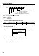
Note The status of the P01/SCK pin is selectable.
Remark (R): Read only
(W): Write only
Serial interface operation enable/disable specification bit (W)
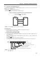
Shift register operation Serial clock counter IRQCSI flag SO/SB0 and SI/SB1 pins
CSIE0 0 Shift operation disabled Cleared Held Used only for port 0
Serial clock selection bit (W)
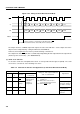
The P01/SCK pin assumes the following state according to the setting of CSIM0 and CSIM1:
CSIM1 CSIM0 P01/SCK pin state
0 0 High impedance
0 1 High level output
10
11
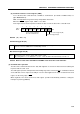
When clearing CSIE during serial transfer, use the following procedure:
<1> Disable interrupts by clearing the interrupt enable flag (IECSI).
<2> Clear CSIE.
<3> Clear the interrupt request flag (IRQCSI).
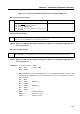
CSIE COI WUP
CSIM4 CSIM3 CSIM2 CSIM1 CSIM0
FE0H
CSIM
76543210
Address
Serial clock selection bit (W)
Note
Serial interface operation mode selection bit (W)
Wake-up function specification bit (W)
Match signal from address comparator (R)
Serial interface operation enable/disable specification bit (W)