
User manual

158
µPD750008 USER'S MANUAL
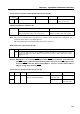
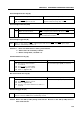
Serial clock selection bit (W)
CSIM1 CSIM0 Serial clock SCK pin mode
0 0 External clock applied to SCK pin Input
0 1 Timer/event counter output (TOUT0) Output
10f
X
/2
4
(262 kHz)
11f
X
/2
3
(524 kHz)
Remark The value at 4.19 MHz is indicated in parentheses.
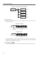
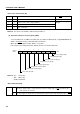
(b) Serial bus interface control register (SBIC)
To use the SBI mode, set SBIC as shown below. (For details on SBIC format, see (2) in Section 5.6.3.)
SBIC is manipulated using a bit manipulation instruction.
When the RESET signal is input, SBIC is set to 00H.
In the figure below, hatched portions indicate the bits used in the SBI mode.
Remark (R): Read only
(W): Write only
(R/W): Read/write
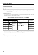
Busy enable bit (R/W)
BSYE 0 <1> The busy signal is automatically disabled.
<2> Busy signal output is stopped in phase with the falling edge of SCK immediately after
clear instruction execution.
1 The busy signal is output after the acknowledge signal in phase with the falling edge of SCK.
BSYE ACKD ACKE ACKT CMDD CMDTRELD RELT
76543 120
Address
SBIC
Bus release trigger bit (W)
FE2H
Command trigger bit (W)
Bus release detection flag (R)
Command detection flag (R)
Acknowledge trigger bit (W)
Acknowledge enable bit (R/W)
Acknowledge detection flag (R)
Busy enable bit (R/W)