
User manual

180
µPD750008 USER'S MANUAL
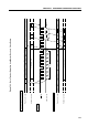
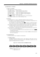
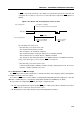
P01/SCK
P01
output
latch
SCK
To internal circuit
Address
FF0H.1
SCK pin output mode
From the serial clock
control circuit
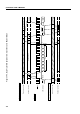
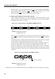
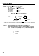
Example To output one SCK/P01 pin clock cycle by software
SEL MB15 ; or CLR1 MBE
MOV XA,#10000011B ; SCK (f
X
/2
3
), output mode
MOV CSIM,XA
CLR1 0FF0H.1 ; SCK/P01 <- 0
SET1 0FF0H.1 ; SCK/P01 <- 1
Figure 5-80. SCK/P01 Pin Circuit Configuration
The P01 output latch is mapped to bit 1 of address FF0H. A RESET signal sets the P01 output latch to
1.
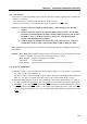
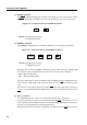
Cautions 1. During normal serial transfer, the P01 output latch must be set to 1.
2. The P01 output latch cannot be addressed by specifying PORT0.1 (as described
below). The address of the latch (0FF0H.1) must be coded in the operand of an
instruction directly. However, MBE = 0 (or MBE = 1, MBS = 15) must be specified
before the instruction is executed.
CLR1 PORT0.1
Not allowed
SET1 PORT0.1
CLR1 0FF0H.1
Allowed
SET1 0FF0H.1