
User manual


4
µPD750008 USER'S MANUAL
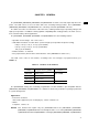
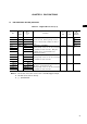
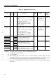
1.3 DIFFERENCES AMONG SUBSERIES PRODUCTS
Item µPD750004 µPD750006 µPD750008 µPD75P0016
Program counter 12 bits 13 bits 14 bits
Program memory (byte) Masked ROM Masked ROM Masked ROM One-time PROM
4096 6144 8192 16384
Data memory (x 4 bits) 512
Mask Pull-up resistors at Incorporated None
option ports 4 and 5 (Whether to incorporate pull-up resistors can (Cannot be
be specified.) incorporated.)
Wait time during Available Not available
RESET (Can be selected from 2
17
/f
X
or 2
15
/f
X
.)
Note
(Fixed to 2
15
/f
X
.)
Selection to use Yes No
feedback resistors (Whether to enable feedback resistors can (Use of feedback
for subsystem clock be specified.) resistors is factory-set)
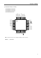
Pin 6-9 (CU) P33-30 P33/MD3-P30/MD0
connection
23-26 (GB)
20 (CU) IC V
PP
38 (GB)
Others Noise immunity and noise radiation vary with the circuit scale and mask
layout.
Note 2
17
/f
X
(21.8 ms at 6.0 MHz, 31.3 ms at 4.19 MHz)
2
15
/f
X
(5.46 ms at 6.0 MHz, 7.81 ms at 4.19 MHz)
Caution The noise immunity and noise radiation of the PROM model differ from those of the mask
ROM model. If you replace the PROM model with the ROM model of the course of
experimental production to mass production, perform thorough evaluation by using the
CS model (not ES model) of the mask ROM model.
*
*