
User manual

11
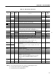
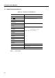
CHAPTER 2 PIN FUNCTIONS
Table 2-2. Non-Port Pin Functions
Input/
Also
Upon
I/O
Pin
output
used Function
reset
circuit
as type
Note 1
TI0 Input P13 Inputs external event pulse to the timer/event counter — B -C
PTO0 I/O P20 Timer/event counter output Input E-B
PTO1 P21 Timer counter output
PCL I/O P22 Clock output Input E-B
BUZ I/O P23 Fixed frequency output Input E-B
(for buzzer or system clock trimming)
SCK I/O P01 Serial clock I/O Input F -A
SO/SB0 I/O P02 Serial data output or serial data bus I/O Input F -B
SI/SB1 I/O P03 Serial data input or serial data bus I/O Input M -C
INT4 Input P00 Edge detection vectored interrupt input — B
(Either a rising or falling edge is detected.)
The INT0/P10 pin has a noise eliminating function.
INT0 Input P10 Edge detection vectored interrupt input Synchronous — B -C
INT1 P11 (The edge to be detected is selectable.) Asynchronous
INT2 Input P12 Rising edge detection testable input Asynchronous — B -C
KR0-KR3 I/O P60-P63 Parallel falling edge detection testable input Input F -A
KR4-KR7 I/O P70-P73 Parallel falling edge detection testable input Input F -A
X1, X2 Input — Connection pin to a crystal/ceramic resonator for main — —
system clock generation.
When external clock is used, it is input to X1,
and its inverted signal is input to X2.
XT1 Input — Connection pin to a crystal for subsystem clock — —
generation.
XT2 — When external clock is used, it is input to XT1, and
XT2 is left open.
RESET Input — System reset input — B
IC
Note 2
— — Internally connected. — —
Connect to V
DD
, keeping the wiring as short as possible.
V
DD
— — Positive power supply — —
V
SS
— — GND potential — —
V
PP
Note 2
— P10/INT0 Program voltage application for program memory — —
(PROM) write/verify operation.
+12.5 V is applied for PROM write/verify operation.
Connect to V
DD
, keeping the wiring as short as
possible.
MD0- I/O P30-P33 Mode selection for program memory (PROM) Input E-B
MD3
Note 3
write/verify operation.
NC — — No connection — —
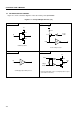
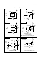
Notes 1. The circuits enclosed in circles have a Schmitt-triggered input.
2. Used as the V
PP
pin for the µPD75P0016.
3. Provided only in the µPD75P0016.
*