
User manual


35
CHAPTER 3 FEATURES OF THE ARCHITECTURE AND MEMORY MAP
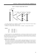
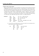
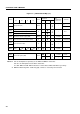
Figure 3-4. Example of Register Bank Selection
The setting of the RBS can be modified for subroutine processing or interrupt processing by saving or
restoring the RBS with the PUSH or POP instruction.
The RBE is set using the SET1 or CLR1 instruction. The RBS is set using the SEL instruction.
Example
SET1 RBE ; RBE <– 1
CLR1 RBE ; RBE <– 0
SEL RB0 ; RBS <– 0
SEL RB3 ; RBS <– 3
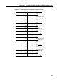
The general register area of the µPD750008 can be used not only on a 4-bit basis, but also on an 8-bit
basis with register pairs. This enables users to perform transfers, arithmetic/logical operations, comparisons,
and increments and decrements at a speed comparable to that of an 8-bit microcomputer, and thereby enables
to program using mainly general registers.
(1) When used as a 4-bit register
When the general register area is used on a 4-bit basis, eight general registers, the X, A, B, C, D, E, H,
and L registers, are available in the register bank specified with RB = RBE·RBS as shown in Figure 3-
5. The A register functions as a 4-bit accumulator which performs transfers, arithmetic/logical operations,
and comparisons. The other general registers perform transfers, comparisons, and increments/decrements
with the accumulator.
SET1 RBE
<Main program>
<Level-one interrupt>
; RBE = 0 in the
vector table
RB = 2
SEL RB2
RB = 0
RB = 1
RETI
<Level-two interrupt>
; RBE = 1 in the
vector table
PUSH BS
SEL RB1
RB = 0
POP BS
RETI
POP rp
RETI
PUSH rp
<Level-three interrupt>
; RBE = 0 in the
vector table