
User manual


36
µPD750008 USER'S MANUAL
(2) When used as an 8-bit register
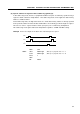
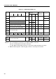
When the general register area is used on an 8-bit basis, the register pairs in the register bank specified
by RBE·RBS can be specified as XA, BC, DE, and HL as shown in Figure 3-6, and the register pairs in
the register bank that has the inverted value of bit 0 of the register bank (RB) can be specified as XA’,
BC’, DE’, and HL’, thus providing up to eight 8-bit registers. The XA register pair functions as an 8-bit
accumulator which performs transfers, arithmetic/logical operations, comparisons, and increments/
decrements of 8-bit data. The other register pairs perform transfers, arithmetic/logical operations,
comparisons, and increments/decrements with the accumulator. The HL register pair functions mainly
as a data pointer, and the DE and DL register pairs function as an auxiliary data pointer.
Examples 1. INCS HL ; HL <– HL + 1, skip at HL = 00H
ADDS XA,BC ; XA <– XA + BC, skip at carry
SUBC DE’,XA ; DE’ <– DE’ – XA – CY
MOV XA,XA’ ; XA <– XA’
MOVT XA,@PCDE ; XA <– (PC
12-8
+ DE) ROM, reference table
SKE XA, BC ; Skip if XA = BC
2. The value of the count register (T0) for timer/event counter 0 is tested until it becomes
greater than the value of the BC’ register pair.
CLR1 MBE
NO: MOV XA,T0 ; Read count register
SUBS XA,BC’ ; XA • BC?
BR YES ; YES
BR NO ; NO