
User manual


56
µPD750008 USER'S MANUAL
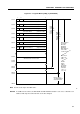
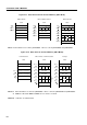
4.5 GENERAL REGISTER: 8 x 4 BITS x 4 BANKS
The general registers are mapped to particular addresses in data memory. Four banks of registers are
provided, with each bank consisting of eight 4-bit registers (B, C, D, E, H, L, X, and A).
The register bank (RB) to be enabled at the time of instruction execution is determined by:
RB = RBE·RBS: (RBS = 0 to 3)
Each general register allows 4-bit manipulation. In addition, BC, DE, HL, or XA serves as a register pair
for 8-bit manipulation. DL also makes a register pair as well as DE and HL. These three register pairs can
be used as data pointers.
In 8-bit manipulation, the register pairs in the register banks (0 <—> 1, 2 <—> 3) that have the inverted
value of bit 0 of the register bank (RB) address can be specified as BC’, DE’, HL’, and XA’ in addition to the
register pairs BC, DE, HL, and XA. (See Section 3.2.)
A general register area can be addressed and accessed as normal RAM, regardless of whether it is used
as a register.
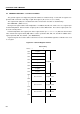
Figure 4-8. General Register Format
Address
000H
001H
002H
003H
004H
005H
006H
007H
008H
00FH
010H
017H
018H
01FH
A register
X register
L register
H register
E register
D register
C register
B register
Same as bank 0
Same as bank 0
Same as bank 0
·································
03
Register bank 0
Register bank 1
Register bank 2
Register bank 3
Data memory