
User manual


60
µPD750008 USER'S MANUAL
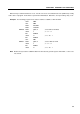
PC11 - PC8
MBE
SP + 2 PC3 - PC0
PC7 - PC4
SP + 4 IST1
CY
SP + 6
SP + 1
SP + 3
SP + 5
Stack
RBE
PC12
IST0
SK2
MBE
SK1
RBE
SK0
RETI instruction
PSW
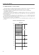
PC11 - PC8
MBE
SP + 2 PC3 - PC0
PC7 - PC4
SP + 4
SP + 1
SP + 3
Stack
RBE
PC12
RET or RETS instruction
Lower bits of pair register
Upper bits of pair register
SP + 2
SP + 1
Stack
POP instruction
SP
SP SP
PC13
Note
PC13
Note
Note Note
Lower bits of pair register
Upper bits of pair register
Stack
PUSH instruction
SP
–
2
SP
–
1
SP
PC11 - PC8
PC3 - PC0
PC7 - PC4
Stack
CALL, CALLA, or CALLF instruction
SP
–
6
SP
–
5
SP
–
4
SP
–
3
SP
–
2
SP
–
1
SP
*
*
*
*
MBE
*
RBE
*
00
PC11 - PC8
PC3 - PC0
PC7 - PC4
Stack
Interrupt
SP
–
6
SP
–
5
SP
–
4
SP
–
3
SP
–
2
SP
–
1
SP
IST1
CY
IST0
SK2
MBE
SK1
RBE
SK0
PSW
00
Note 2
PC12
PC12PC13PC13
Note 1
Note 1
Note 1 Note 1
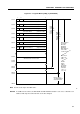
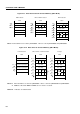
Figure 4-13. Data Restored from the Stack Memory (Mk I Mode)
Note PC12 and PC13 are 0 in the µPD750004. PC13 is 0 in the µPD750006 and µPD750008.
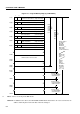
Figure 4-14. Data Saved to the Stack Memory (Mk II Mode)
Notes 1. PC12 and PC13 are 0 in the µPD750004. PC13 is 0 in the µPD750006 and µPD750008.
2. PSW bits other than MBE and RBE are not saved or restored.
Remark * indicates an undefined bit.