
User's Manual

106
µPD750008 USER'S MANUAL
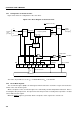
5.4.1 Configuration of the Clock Timer
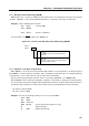
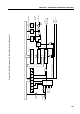
Figure 5-26 shows the configuration of the clock timer.
Figure 5-26. Block Diagram of the Clock Timer
The values in parentheses are for f
X
= 4.194304 MHz and f
XT
= 32.768 kHz.
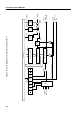
5.4.2 Clock Mode Register
The clock mode register (WM) is an 8-bit register which controls the clock timer. Figure 5-27 shows the
format of the clock mode register.
All bits except bit 3 of the clock mode register are controlled by an 8-bit manipulation instruction. Bit 3 is
for testing the XT1 pin input level. The input level of the XT1 pin can be tested by bit test operation. No data
can be written to this register.
When the RESET signal is generated, all bits except bit 3 of this register are cleared to 0.
P23/BUZ
Internal bus
8
Selector
From the
clock
generator
f
X
128
(32.768 kHz)
f
XT
(32.768 kHz)
Selector Frequency divider
Selector
INTW
IRQW
set signal
2 Hz
0.5 sec
WM7 0 WM5 WM4 WM3 WM2 WM1 WM0
P23 output
latch
Bit 2 of PMGBPORT2.3
Output buffer
Clear signal
f
W
(32.768 kHz)
Bit test instruction
Port 2 input/
output mode
WM
(4 kHz) (2 kHz)
f
w
2
7
(256 Hz: 3.91 ms)
f
w
2
14
f
w
2
3
f
w
2
4