
User's Manual

125
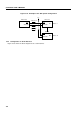
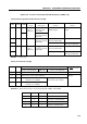
CHAPTER 5 PERIPHERAL HARDWARE FUNCTIONS
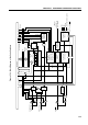
Figure 5-39. Block Diagram of the Serial Interface
Internal bus
88
8
8/4
P03/SI0/SB1
P02/SO0/SB0
P01/SCK
(8)
f
x
/2
3
f
x
/2
4
f
x
/2
6
TOUT0
(from timer/event counter)
CSIM
RELD
CMDD
ACKD
ACKT
ACKE
BSYE
RELT
CMDT
DQ
SET CLR
(8)
(8)
SBIC
Bit
test
Slave address register (SVA)
Address comparator
Match
signal
Bit manipulation
SO latch
Bit test
Selec-
tor
Selec-
tor
Busy/
acknowledge
output circuit
Bus release/
command/
acknowledge
detection circuit
Serial clock
counter
Serial clock
control circuit
INTCSI
control circuit
IRQCSI
set signal
INTCSI
P01
output latch
Serial clock
selector
External SCK
Shift register (SIO)