
User's Manual

130
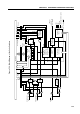
µPD750008 USER'S MANUAL
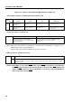
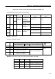
Figure 5-40. Format of Serial Operation Mode Register (CSIM) (4/4)
Remarks 2. The P01/SCK pin assumes any of the following states according to the state of
CSIE, CSIM1, and CSIM0:
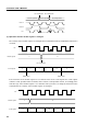
CSIE CSIM1 CSIM0 P01/SCK pin state
0 0 0 Input port
1 0 0 High impedance
0 0 1 High level output
010
011
1 0 1 Serial clock output (High level output)
110
111
3. When clearing CSIE during serial transfer, use the following procedure:
<1> Disable interrupts by clearing the interrupt enable flag (IECSI).
<2> Clear CSIE.
<3> Clear the interrupt request flag (IRQCSI).
Examples 1. f
X
/2
4
is selected as the serial clock, serial interrupt IRQCSI, is generated each
time serial transfer is completed, and serial transfer is performed in the SBI
mode with the SB0 pin used as the serial data bus.
SEL MB15 ; or CLR1 MBE
MOV XA,#10001010B
MOV CSIM,XA ; CSIM <– 10001010B
2. Serial transfer dependent on the contents of CSIM is enabled.
SEL MB15 ; or CLR1 MBE
SET1 CSIE