
User's Manual

147
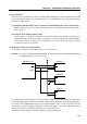
CHAPTER 5 PERIPHERAL HARDWARE FUNCTIONS
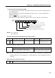
Bus release trigger bit (W)
RELT Control bit for bus release signal (REL) trigger output.
By setting RELT = 1, the SO latch is set to 1. Then the RELT bit automatically cleared to 0.
Caution Never use bits other than RELT and CMDT in the two-wire serial I/O mode.
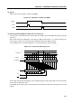
(2) Communication operation
The two-wire serial I/O mode transfers data, with eight bits as one block. Data is transferred bit by bit
in phase with the serial clock.
The shift register performs shift operation on the falling edge of the serial clock (SCK). Transmit data is
latched on the SO latch, and is output on the SB0/P02 pin or SB1/P03 pin starting with the MSB. Receive
data applied to the SB0 pin or SB1 pin is latched in the shift register on the rising edge of SCK.
When eight bits have been transferred, shift register operation automatically terminates setting the
interrupt request flag (IRQCSI).
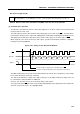
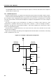
Figure 5-48. Timing of Two-Wire Serial I/O Mode
The SB0 (or SB1) pin becomes an N-ch open-drain I/O when specified as the serial data bus, so the voltage
level on that pin must be pulled up externally.
The state of the SO latch is output on the SB0 (or SB1) pin, so the SB0 (or SB1) pin output states can
be controlled by setting the RELT or CMDT bit.
However, this operation must not be performed during serial transfer.
The output state of the SCK pin can be controlled by manipulating the P01 output latch in the output mode
(internal system clock mode). (See Section 5.6.8.)
SCK
SB0, SB1
IRQCSI
1 2345678
D0D1D2D3D4D5D6D7
Transfer operation is started in phase with falling edge of SCK.
Execution of instruction that writes date to SIO (Transfer start request)
Completion of transfer