
User's Manual


230
µPD75008 USER'S MANUAL
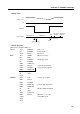
9.1 OPERATING MODES WHEN WRITING TO AND VERIFYING THE PROGRAM MEMORY
If +6 V is applied to the VDD pin and +12.5 V is applied to the V
PP
pin, the µPD75P0016 enters program
memory write/verify mode. The specific operating mode is then selected by the setting of the MD0 through
MD3 pins as listed in the table below.
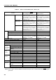
Operating mode specification
Operating mode
V
PP
V
DD
MD0 MD1 MD2 MD3
+12.5 V +6 V H L H L Program memory address clear mode
L H H H Write mode
L L H H Verify mode
H X H H Program inhibit mode
Remark X indicates L or H.
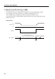
9.2 WRITING TO THE PROGRAM MEMORY
The procedure for writing to program memory is described below; high-speed write is possible.
(1) Pull low all unused pins to V
SS
by means of resistors.
Bring X1 to low level.
(2) Apply 5 V to V
DD
and to V
PP
.
(3) Wait 10 µs.
(4) Select program memory address clear mode.
(5) Apply 6 V to V
DD
and 12.5 V to V
PP
.
(6) Select program inhibit mode.
(7) Select write mode for 1 ms duration and write data.
(8) Select program inhibit mode.
(9) Select verify mode. If write is successful, proceed to step (10). If write fails, repeat steps (7) to (9).
(10) Perform additional write for (Number of repetitions of steps (7) to (9)) x 1 ms duration.
(11) Select program inhibit mode.
(12) Increment the program memory address by inputting four pulses on the X1 pin.
(13) Repeat steps (7) to (12) until the last address is reached.
(14) Select program memory address clear mode.
(15) Apply 5 V to V
DD
and to V
PP
.
(16) Turn the power off.