
User's Manual

20
µPD750008 USER'S MANUAL
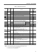
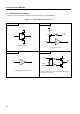
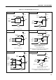
2.4 CONNECTION OF UNUSED PINS
Table 2-3. Connection of Unused Pins
Pin name Recommended connection
P00/INT4 To be connected to V
SS
P01/SCK To be connected to V
SS
or V
DD
P02/SO/SB0
P03/SI/SB1
P10/INT0-P12/INT2 To be connected to V
SS
P13/TI0
P20/PTO0 Input state: To be connected to V
SS
or
P21/PTO1 V
DD
through a resistor
P22/PCL Output state: To be left open
P23/BUZ
P30(/MD0)-P33(/MD3)
Note
P40-P43
P50-P53
P60-P63
P70-P73
P80-P81
XT1 To be connected to V
SS
or V
DD
XT2 To be left open
IC (V
PP
)
Note
To be connected directly to V
DD
Note ( ): µPD75P0016