
User's Manual


21
CHAPTER 3 FEATURES OF THE ARCHITECTURE AND MEMORY MAP
CHAPTER 3 FEATURES OF THE ARCHITECTURE AND MEMORY MAP
The 75XL series architecture of the µPD750008 has the following features:
• Internal RAM of up to 4K words x 4 bits (12-bit address)
• Peripheral hardware expansibility
To provide these features, the following are used:
(1) Data memory bank structure
(2) General register bank structure
(3) Memory-mapped I/O
This chapter explains these topics.
3.1 DATA MEMORY BANK STRUCTURE AND ADDRESSING MODES
3.1.1 Data Memory Bank Structure
In the µPD750008, addresses 000H to 1FFH in data memory space are assigned to static RAM (512 words
x 4 bits), and addresses F80H to FFFH are assigned to peripheral hardware (such as I/O ports and timers).
To address a 12-bit location in this data memory space (4K x 4 bits), the µPD750008 uses such a memory
bank structure that the low-order eight bits are specified with an instruction directly or indirectly, and the high-
order four bits are used to specify a memory bank.
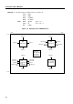
To specify a memory bank (MB), two hardware items are incorporated:
• Memory bank enable flag (MBE)
• Memory bank select register (MBS)
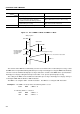
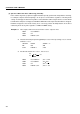
The MBS is a register used to select a memory bank, and the register can be set to 0, 1, or 15. The MBE
is a flag used to determine whether the memory bank selected using the MBS is valid. As shown in Figure
3-1, when the MBE is set to 0, a certain memory bank is always selected regardless of the setting of the MBS.
When the MBE is set to 1, memory bank selection depends on the setting of the MBS, thus enabling data
memory space expansion.
In addressing data memory space, the MBE is usually set to 1 (MBE = 1), and data memory in the memory
bank specified in the MBS is operated. However, the MBE = 0 mode or MBE = 1 mode can be selected for
each step of processing for more efficient programming.
3