
User's Manual

59
CHAPTER 4 INTERNAL CPU FUNCTIONS
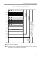
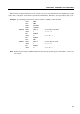
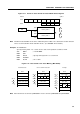
Figure 4-11. Format of Stack Pointer and Stack Bank Select Register
Note The Mk I mode and Mk II mode can be switched by bit 3 of SBS. The stack bank selection function
can be used in both Mk I mode and Mk II mode. (See Section 4.1 for details.)
Example SP initialization
Specify memory bank 1 as a stack area to start stack operation at address 1FFH.
SEL MB15 ; or CLR1 MBE
MOV A,#1
MOV SBS,A ; Specify memory bank 1 as a stack area
MOV XA,#00H
MOV SP,XA ; SP <– 00H
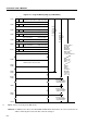
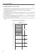
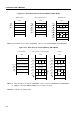
Figure 4-12. Data Saved to the Stack Memory (Mk I Mode)
Note PC12 and PC13 are 0 in the µPD750004. PC13 is 0 in the µPD750006 and µPD750008.
SP
SP
SP7 SP6 SP5 SP4 SP3 SP2 SP1 0
SBS0
SBS10
SBS3
SP
SBS
Symbol
F80H
F84H
Address
SBS
0FFH
100H
000H
1FFH
Memory bank 0
Memory bank 1
Note
SP – 6 PC11 - PC8
MBE
SP – 4 PC3 - PC0
PC7 - PC4
SP – 2 IST1
CY
SP – 5
SP – 3
SP – 1
Stack
RBE
PC12
IST0
SK2
MBE
SK1
RBE
SK0
Interrupt
PSW
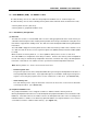
SP – 4 PC11 - PC8
MBE
SP – 2 PC3 - PC0
PC7 - PC4
SP – 3
SP – 1
Stack
RBE
PC13 PC12
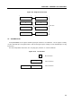
CALL or CALLF instruction
SP – 2
Lower bits of pair register
Upper bits of pair register
SP
SP – 1
Stack
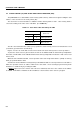
PUSH instruction
Note
SP
SP
Note
PC13
Note
Note