
Electronics America Personal Computer User Manual

µ
PD75P308
11
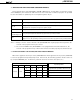
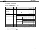
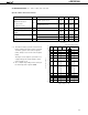
Pin Name Function
VPP Applies voltage when program memory is written/verified (normally, at VDD potential)
These pins input clock that updates address when program memory is written/verified. To X2 pin,
input signal 180º out of phase in respect to signal to X1 pin.
MD0-MD3 These pins select operation mode when program memory is written/verified.
P40-P43 (Lower 4)
P50-P53 (Upper 4)
Power supply voltage application pin.
Apply 5V ± 5% to this pin during normal operation and 6V when program memory is written/verified.
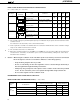
3. WRITING AND VERIFYING PROM (PROGRAM MEMORY)
The program memory of the
µ
PD75P308 is a PROM of 8064 x 8 bits. To write data to or verify the contents
of this PROM, the pins listed in the table below are used. Note that no address input pins are provided
because the address is updated by the clock input through the X1 pin.
These pins input/output 8-bit data when program memory is written/verified.
VDD
X1, X2
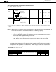
Note 1:
Always cover the erasure window of the
µ
PD75P308K with a light-opaque film except when the
contents of the program memory are erased.
2:
The one-time PROM model
µ
PD75P308GF is not equipped with a window and therefore, the
contents of the program memory of this model cannot be erased by exposing it to ultraviolet rays.
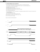
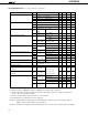
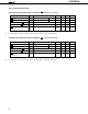
3.1 OPERATION MODES FOR WRITING/VERIFYING PROGRAM MEMORY
When +6V is applied to the V
DD pin of the
µ
PD75P308 with +12.5V applied to the VPP pin, the
µ
PD75P308
is set in the program memory write/verify mode. In this mode, the following operation modes can be set
by using the MD0-MD3 pins. At this time, pull down the levels of all the other pins to VSS.
Operating Mode Specification
MD0 MD1 MD2 MD3
HLHL
LHHH
LLHH
HxHH
VDD
+6 V
VPP
+12.5 V
Operating Mode
Program memory address 0 clear mode
Write mode
Verify mode
Program inhibit mode
x: L or H