
Electronics America Personal Computer User Manual

µ
PD75P308
17
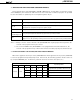
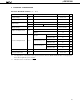
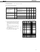
32 32.768 35 kHz
1.0 2 s
32 100 kHz
515
µ
s
Crystal Oscillation
frequency (fXT)
Oscillation stabilization
time
*
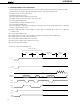
External Clock XT1 input frequency
(fXT)
XT1 input high-, low-level
widths (tXTH, tXTL)
SUBSYSTEM CLOCK OSCILLATOR CIRCUIT CHARACTERISTICS
(T
a = -10 to +70°C, VDD = 5 V ±5%)
Oscillator Item Conditions MIN. TYP. MAX. Unit
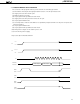
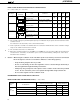
Recommended
Constants
XT1 XT2
R
C3 C4
V
DD
XT1 XT2
Open
*: Time required for oscillation to stabilize after VDD reaches the minimum value of the oscillation voltage
range.
Caution: When using the oscillation circuit of the subsystem clock, wire the portion enclosed in dotted line
in the figures as follows to avoid adverse influences on the wiring capacity:
• Keep the wiring length as short as possible.
• Do not cross the wiring over the other signal lines. Do not route the wiring in the vicinity of
lines through which a high alternating current flows.
• Always keep the ground point of the capacitor of the oscillator circuit at the same potential
as V
DD. Do not connect the power source pattern through which a high current flows.
• Do not extract signals from the oscillation circuit.
The amplification factor of the subsystem clock oscillation circuit is designed to be low to reduce the
current dissipation and therefore, the subsystem clock oscillation circuit is influenced by noise more
easily than the main system clock oscillation circuit. When using the subsystem clock, therefore,
exercise utmost care in wiring the circuit.
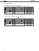
CAPACITANCE (T
a = 25°C, VDD = 0 V)
Parameter Symbol Conditions MIN. TYP. MAX. Unit
Input Capacitance CIN f = 1 MHz 15 pF
Output Capacitance COUT Pins other than thosemeasured are at 0 V 15 pF
Input/Output CIO
15 pF
Capacitance
★