
Electronics America 4-Bit Single-Chip Microcomputer User's Manual

CHAPTER 3. FEATURES OF ARCHITECTURE AND MEMORY MAP
29
W
W
Bit 2 is fixed to 0.
W
W
R/W R/W
R/W R/W
R/W R/W
R/W R/W
FB2H
FB3H
FB4H
FB8H
FBDH
FBEH
FBFH
Bit 0 is fixed to 0.
F80H
F85H
F86H
W
b3 b2 b1 b0
Stack pointer (SP)
Basic interval timer mode register (BTM)
Basic interval timer (BT)
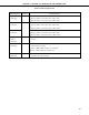
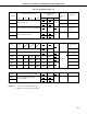
Table 3-4
µ
PD75402A I/O Map (1/2)
Address
1 Bit 4 Bits 8 Bits
Remarks
Bit
Manipula-
tion
No. of Manipulatable
Addressing
Hardware Name (Symbol)
W
11 must always
be written in
bit 1, 0.
R
(IME)
Processor clock control register (PCC)
INT0 mode register (IM0)
0 0 IEBT IRQBT
0 0 IECSI IRQCSI
0 0 IE0 IRQ0
0 0 IE2 IRQ2
Manipulation
by EI. DI instruc-
tion
FD0H
FDCH
Clock output mode register (CLOM)
Pull-up resistor specify register
Group A (POGA)
fmem. bit
Remarks 1. IE××× is an interrupt enable flag.
2. IRQ××× is an interrupt request flag.