
Electronics America 4-Bit Single-Chip Microcomputer User's Manual

88
CHAPTER 5. PERIPHERAL HARDWARE FUNCTIONS
(2) Communication operation
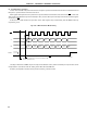
In the 3-wire serial I/O mode, data transmission/ reception is performed in 8-bit units. Data is transmitted/received
bit by bit in synchronization with the serial clock.
Shift register shift operations are performed in synchronization with the fall of the serial clock (SCK). Then send
data is held in the SO latch output from the SO pin. Also, receive data input to the SI pin is latched in the shift register
on the rise of SCK.
At the end of an 8-bit transfer the operation of the shift register stops automatically and the IRQCSI interrupt
request flag is set.
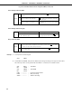
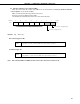
Fig. 5-29 3-Wire Serial I/O Mode Timing
The SO pin becomes a CMOS output and outputs the SO latch status, and thus the SO pin output status can be
manipulated in accordance with the setting of the RELT bit and CMDT bit.
However, manipulation should not be performed during a serial transfer.
SCK
SI
SO
IRQCSI
Start of Transfer Symchronized with Fall of SCK
Execution of Instruction which Writes Data to SIO
(Trasfer Start Directive)
End of
Transfer
1 2 3 4 5 6 7 8
DI7 DI6 DI5 DI4 DI3 DI2 DI1 DI0
DO7 DO6 DO5 DO4
DO3
DO2 DO1 DO0