
Single-Chip Microcontrollers User's Manual


558
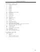
CHAPTER 27 INSTRUCTION SET
Clock Flag
Note 1 Note 2
ZACCY
(SP – 1) ← (PC + 3)H, (SP – 2) ← (PC + 3)L,
PC ← addr16, SP ← SP – 2
(SP – 1) ← (PC + 2)H, (SP – 2) ← (PC + 2)L,
CALLF !addr11 2 5 – PC15 – 11 ← 00001, PC10 – 0 ← addr11,
SP ← SP – 2
(SP – 1) ← (PC + 1)H, (SP – 2) ← (PC + 1)L,
PCH ← (00000000, addr5 + 1),
PCL ← (00000000, addr5),
SP ← SP – 2
(SP – 1) ← PSW, (SP – 2) ← (PC + 1)H,
BRK 1 6 – (SP – 3) ← (PC + 1)L, PCH ← (003FH),
PCL ← (003EH), SP ← SP – 3, IE ← 0
PCH ← (SP + 1), PCL ← (SP),
SP ← SP + 2
PCH ← (SP + 1), PCL ← (SP),
RETI 1 6 – PSW ← (SP + 2), SP ← SP + 3, R R R
NMIS ← 0
PCH ← (SP + 1), PCL ← (SP),
PSW ← (SP + 2), SP ← SP + 3
PSW 1 2 – (SP – 1) ← PSW, SP ← SP – 1
(SP – 1) ← rpH, (SP – 2) ← rpL,
SP ← SP – 2
PSW 1 2 – PSW ← (SP), SP ← SP + 1 R R R
rpH ← (SP + 1), rpL ← (SP),
SP ← SP + 2
SP, #word 4 – 10 SP ← word
MOVW SP, AX 2 – 8 SP ← AX
AX, SP 2 – 8 AX ← SP
!addr16 3 6 – PC ← addr16
BR $addr16 2 6 – PC ← PC + 2 + jdisp8
AX 2 8 – PCH ← A, PCL ← X
BC $addr16 2 6 – PC ← PC + 2 + jdisp8 if CY = 1
BNC $addr16 2 6 – PC ← PC + 2 + jdisp8 if CY = 0
BZ $addr16 2 6 – PC ← PC + 2 + jdisp8 if Z = 1
BNZ $addr16 2 6 – PC ← PC + 2 + jdisp8 if Z = 0
Notes 1. When the internal high-speed RAM area is accessed or instruction with no data access
2. When an area except the internal high-speed RAM area is accessed
Remarks 1. One instruction clock is the length of 1 clock cycle of the CPU clock (f
CPU) selected by the processor
clock control register (PCC).
2. This clock cycle applies to internal ROM program.
3. n is the number of waits when external memory expansion area is read from.
4. m is the number of waits when external memory expansion area is written to.
Mnemonic Operands Byte Operation
Instruction
Group
CALL !addr16 3 7 –
CALLT [addr5] 1 6 –
RETB 16 – RRR
RET 16 –
rp 1 4 –
rp 1 4 –
PUSH
POP
Uncondi-
tional
branch
Stack
manipu-
late
Conditional
branch
Call/return