
Single-Chip Microcontrollers User's Manual


475
CHAPTER 20 SERIAL INTERFACE CHANNEL 2
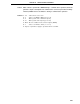
Caution When a write is performed to BRGC during a communication operation, baud rate
generator output is disrupted and communication cannot be performed normally.
Therefore, BRGC must not be written to during a communication operation.
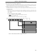
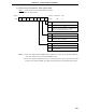
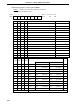
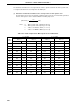
Remarks 1. f
SCK : 5-bit counter source clock
2. k : Value set in MDL0 to MDL3 (0 ≤ k ≤ 14)
3. fX : Main system clock oscillation frequency
4. f
XX : Main system clock frequency (fX or fX/2)
5. MCS : Bit 0 of oscillation mode selection register (OSMS)
6. n : Value set in TPS0 to TPS3 (1 ≤ n ≤ 11)
7. Figures in parentheses apply to operation with f
X = 5.0 MHz.