
Single-Chip Microcontrollers User's Manual


541
CHAPTER 23 EXTERNAL DEVICE EXPANSION FUNCTION
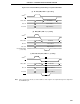
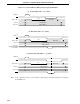
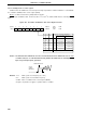
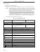
Figure 23-10. External Memory Read Timing in Separate Bus Mode
(a) No wait (PW1, PW0 = 0, 0) setting
(b) Wait (PW1, PW0 = 0, 1) setting
(c) External wait (PW1, PW0 = 1, 1) setting
Note In the separate bus mode, use of the address strobe signal is not required though it is output from
the ASTB/P67 pin.
ASTB
Note
RD
AD0 to AD7
A0 to A7
A8 to A15
Lower Address
Read Data
Higher Address
Lower Address
ASTB
Note
RD
AD0 to AD7
A0 to A7
A8 to A15
Lower Address
Read Data
Higher Address
Lower Address
Internal Wait Signal
(1-clock wait)
ASTB
Note
RD
Lower Address
Read Data
Higher Address
Lower Address
AD0 to AD7
A0 to A7
A8 to A15
WAIT