
Single-Chip Microcontrollers User's Manual


542
CHAPTER 23 EXTERNAL DEVICE EXPANSION FUNCTION
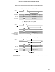
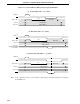
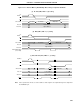
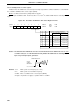
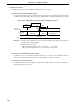
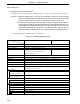
Figure 23-11. External Memory Write Timing in Separate Bus Mode
(a) No wait (PW1, PW0 = 0, 0) setting
(b) Wait (PW1, PW0 = 0, 1) setting
(c) External wait (PW1, PW0 = 1, 1) setting
Note In the separate bus mode, use of the address strobe signal is not required though it is output from
the ASTB/P67 pin.
ASTB
Note
WR
AD0 to AD7
A0 to A7
A8 to A15
Lower Address
Write Data
Higher Address
Lower Address
Hi-Z
ASTB
Note
WR
AD0 to AD7
A0 to A7
A8 to A15
Lower Address
Write Data
Higher Address
Lower Address
Internal Wait Signal
(1-clock wait)
Hi-Z
ASTB
Note
WR
Higher Address
Lower Address
AD0 to AD7
A0 to A7
A8 to A15
WAIT
Hi-Z
Lower Address
Write Data