
Single-Chip Microcontrollers User's Manual


578
CHAPTER 27
µ
PD78P078, 78P078Y
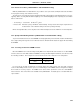
27.3.3 PROM reading procedure
PROM contents can be read onto the external data bus (D0 to D7) using the following procedure.
(1) Fix the RESET pin low, and supply +5 V to the V
PP pin. Unused pins are handled as shown in, 1.5 (2) PROM
programming mode and 2.5 Pin Configuration (Top View).
(2) Supply +5 V to the V
DD and VPP pins.
(3) Input address of data to be read to pins A0 through A16.
(4) Read mode.
(5) Output data to pins D0 through D7.
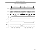
The timing for steps (2) through (5) above is shown in Figure 27-7.
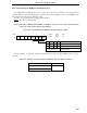
Figure 27-7. PROM Read Timing
Address InputA0 to A16
CE (Input)
OE (Input)
D0 to D7
Hi-Z
Hi-Z
Data output