
Electronics America Single-Chip Microcontrollers User's Manual

CHAPTER 10 10-BIT A/D CONVERTER
User’s Manual U15331EJ4V1UD
175
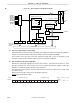
(3) Sample & hold circuit
The sample & hold circuit samples consecutive analog inputs from the input circuit, one by one, and sends
them to the voltage comparator. The sampled analog input voltage is held during A/D conversion.
(4) Voltage comparator
The voltage comparator compares an analog input with the voltage output by the series resistor string.
(5) Series resistor string
The series resistor string is configured between AV
DD and AVSS. It generates the reference voltages against
which analog inputs are compared.
(6) ANI0 to ANI7
The ANI0 to ANI7 pins are the 8-channel analog input pins for the A/D converter. They are used to receive
the analog signals for A/D conversion.
Caution Do not supply the ANI0 to ANI7 pins with voltages that fall outside the rated range. If a
voltage greater than or equal to AV
DD or less than or equal to AVSS (even if within the
absolute maximum rating) is applied to any of these pins, the conversion value for the
corresponding channel will be undefined. Furthermore, the conversion values for the other
channels may also be affected.
(7) AV
SS pin
The AVSS pin is the ground potential pin for the A/D converter. This pin must be held at the same potential as
the V
SS pin, even while the A/D converter is not being used.
(8) AVDD pin
The AVDD pin is the analog power supply pin for the A/D converter. This pin must be held at the same
potential as the V
DD pin, even while the A/D converter is not being used.
(9) Band-gap circuit
The band-gap circuit activates the reference voltage inside the comparator prior to A/D conversion. Start
conversion after 14
µ
s have elapsed following the activation of the band-gap circuit.