
Electronics America Single-Chip Microcontrollers User's Manual

CHAPTER 10 10-BIT A/D CONVERTER
User’s Manual U15331EJ4V1UD
177
Cautions 1. Start conversion (ADCS0 = 1) after 14
µ
s have elapsed following the setting of ADCE0.
If ADCE0 is not used, the conversion result immediately after the setting of bit 7 (ADCS0)
is undefined.
2. The conversion result may be undefined after ADCS0 has been cleared to 0. To read the
conversion result, perform the read operation during A/D conversion. If the conversion
result needs to be read after A/D conversion has been stopped, stop the A/D conversion
operation before the end of the next A/D conversion.
3. Always set bits 1, 2, and 6 to 0.
Remarks 1. f
X: Main system clock oscillation frequency
2. The parenthesized values apply to operation at fX = 5.0 MHz.
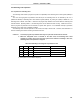
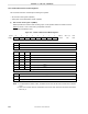
(2) Analog input channel specification register 0 (ADS0)
ADS0 specifies the port used to input the analog voltage to be converted to a digital signal.
ADS0 is set with a 1-bit or 8-bit memory manipulation instruction.
RESET input clears ADS0 to 00H.
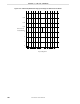
Figure 10-3. Format of Analog Input Channel Specification Register 0
0 0 0 0 0 ADS02 ADS01 ADS00ADS0
Symbol Address After reset R/W
FF84H 00H R/W
76543210
Analog input channel specification
ADS02
0
0
0
0
1
1
1
1
ANI0
ANI1
ANI2
ANI3
ANI4
ANI5
ANI6
ANI7
ADS01
0
0
1
1
0
0
1
1
ADS00
0
1
0
1
0
1
0
1
Caution Bits 3 to 7 must be set to 0.