
Electronics America Single-Chip Microcontrollers User's Manual

CHAPTER 12 SERIAL INTERFACE 1A0
User’s Manual U15331EJ4V1UD 223
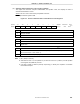
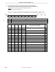
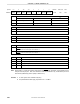
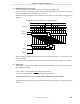
Figure 12-4. Format of Automatic Data Transmit/Receive Interval Specification Register 0 (2/2)
Symbol <7> 6 5 <4> <3> <2> <1> <0> Address After reset R/W
ADTI0 ADTI07 0 0 ADTI04 ADTI03 ADTI02 ADTI01 ADTI00 FF7BH 00H R/W
ADTI04 ADTI03 ADTI02 ADTI01 ADTI00 Data transfer interval specification
(f
X = 5.0 MHz, fSCK = 1.25 MHz)
Note 2
n
1 0 0 0 0 13.6
µ
s + 0.5/fSCK 16
1 0 0 0 1 14.4
µ
s + 0.5/fSCK 17
1 0 0 1 0 15.2
µ
s + 0.5/fSCK 18
1 0 0 1 1 16.0
µ
s + 0.5/fSCK 19
1 0 1 0 0 16.8
µ
s + 0.5/fSCK 20
1 0 1 0 1 17.6
µ
s + 0.5/fSCK 21
1 0 1 1 0 18.4
µ
s + 0.5/fSCK 22
1 0 1 1 1 19.2
µ
s + 0.5/fSCK 23
1 1 0 0 0 20.0
µ
s + 0.5/fSCK 24
1 1 0 0 1 20.8
µ
s + 0.5/fSCK 25
1 1 0 1 0 21.6
µ
s + 0.5/fSCK 26
1 1 0 1 1 22.4
µ
s + 0.5/fSCK 27
1 1 1 0 0 23.2
µ
s + 0.5/fSCK 28
1 1 1 0 1 24.0
µ
s + 0.5/fSCK 29
1 1 1 1 0 24.8
µ
s + 0.5/fSCK 30
1 1 1 1 1 25.6
µ
s + 0.5/fSCK 31
Notes 1. The interval time depends only on the CPU processing.
2. The data transfer interval time is found from the following expressions (n: Value set to ADTI00 to
ADTI04).
<1> n = 0
Interval time = +
<2> n = 1 to 31
Interval time = +
Cautions 1. Do not write to ADTI0 during operation of the automatic transmit/receive function.
2. Be sure to set bits 5 and 6 to 0.
Remark f
X: Main system clock oscillation frequency
fSCK: Serial clock frequency
2
fSCK
0.5
f
SCK
n+1
f
SCK
0.5
f
SCK