
Electronics America Single-Chip Microcontrollers User's Manual

CHAPTER 12 SERIAL INTERFACE 1A0
226 User’s Manual U15331EJ4V1UD
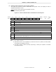
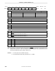
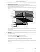
Symbol <7> 6 <5> <4> 3 2 1 0 Address After reset R/W
CSIM1A0 CSIE10 DIR10 ATE0 LSCK10 0 0 SCL101 SCL100 FF78H 00H R/W
Specification of operation enable/disable
CSIE10
Shift register operation Serial counter Port
Note
0 Operation stopped Cleared Port function
1 Operation enabled Count operation enabled Serial function + port function
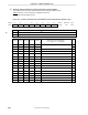
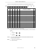
DIR10 Specification of first bit of serial transfer data
0 MSB
1 LSB
ATE0 Selection of operation mode
0 3-wire serial mode
1 3-wire serial mode with automatic transmit/receive function
LSCK10 Chip enable control of SCK10 pin
0 SCK10 is used as port (P23) when CSIE10 = 0.
SCK10 is used for clock output when CSIE10 = 1.
1 SCK10 is fixed to high-level output when CSIE10 = 0.
SCK10 is used for clock output when CSIE10 = 1.
SCL101 SCL100 Selection of serial clock
0 0 External clock input to SCK10 pin
0 1 fX/2
2
(1.25 MHz)
1 0 fX/2
3
(625 kHz)
1 1 fX/2
4
(313 kHz)
Note When CSIE10 = 0 (SIO1A0 operation stop status), the SCK10/P23, SO10/P24, and SI10/P25 pins can
freely be used as port pins. Also, when CSIE10 is used for transmission only, the SI10/P25 pin can be
used as P25 (CMOS I/O) (set bit 7 (RE0) of ADTC0 to 0).
Remarks 1. f
X: Main system clock oscillation frequency
2. The parenthesized values apply to operation at f
X = 5.0 MHz.