
Electronics America Single-Chip Microcontrollers User's Manual

CHAPTER 12 SERIAL INTERFACE 1A0
User’s Manual U15331EJ4V1UD 229
(3) MSB/LSB switching as the start bit
In the 3-wire serial I/O mode, transfer can be selected to start from the MSB or LSB.
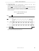
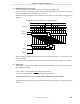
Figure 12-6 shows the configuration of serial I/O shift register 1A0 (SIO1A0) and the internal bus. As shown
in the figure, MSB/LSB can be read/written in reverse form.
MSB/LSB switching as the start bit can be specified with bit 6 (DIR10) of serial operation mode register 1A0
(CSIM1A0).
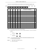
Figure 12-6. Circuit of Switching in Transfer Bit Order
7
6
Internal bus
1
0
LSB-first
MSB-first
Read/write gate
SI10
Shift I/O shift register 1A0 (SIO1A0)
Read/write gate
SO10
SCK10
DQ
SO1 latch
Start bit switching is realized by switching the bit order for data write to SIO1A0. The SIO1A0 shift order
remains unchanged.
Thus, switching between MSB-first and LSB-first must be performed before writing data to the shift register.
(4) Transfer start
Serial transfer is started by setting transfer data to serial I/O shift register 1A0 (SIO1A0) when the following
two conditions are satisfied.
• Bit 7 (CSIE10) of serial operation mode register 1A0 (CSIM1A0) = 1
• Internal serial clock is stopped or SCK10 is high after 8-bit serial transfer.
Caution If CSIE10 is set to “1” after data is written to SIO1A0, transfer does not start.
Termination of 8-bit transfer stops the serial transfer automatically and generates the interrupt request signal
(INTCSI10).